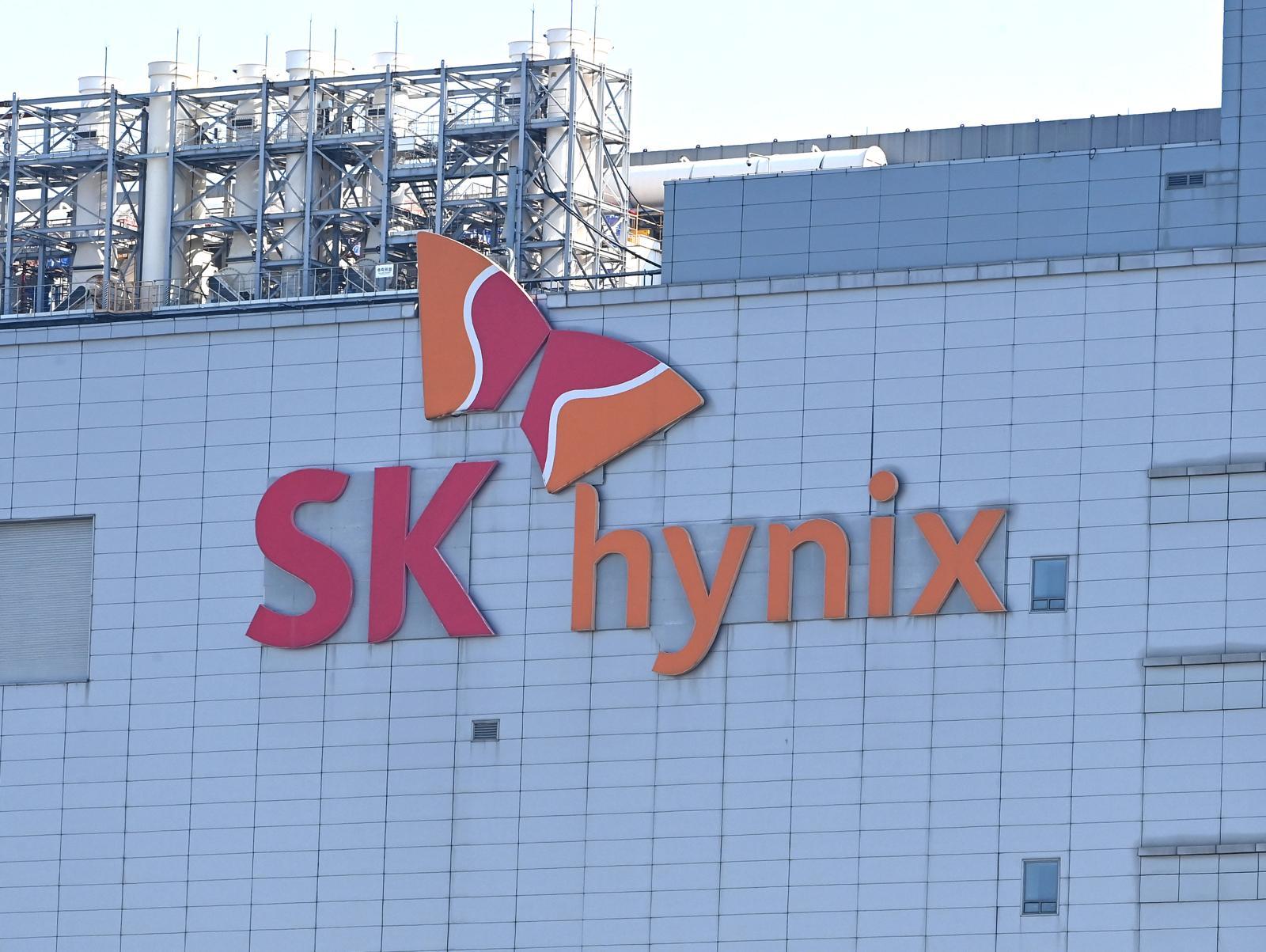
On-site at the groundbreaking of a semiconductor fab in Indiana, USA
Targeting mass production in three years with a USD 4 billion investment
About 100 Korean materials, parts, and equipment firms to enter the local market… expected to create some 7,000 direct and indirect jobs
Industry-academia partnership with Purdue University, which has a cleanroom… aims to train 150 semiconductor specialists within two years
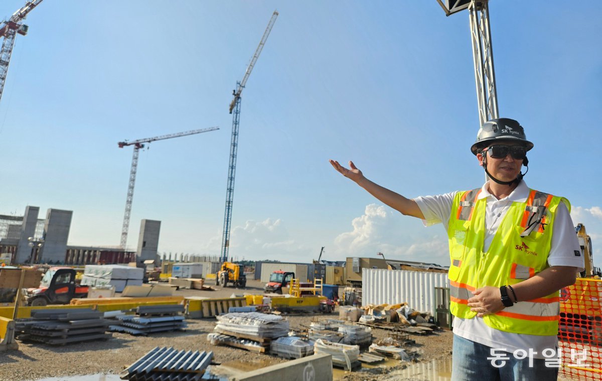
On August 26 (local time), SK hynix Construction Team Leader Kim Hyun-jung explains the construction progress at the site of the semiconductor plant under construction in West Lafayette, Indiana, United States. West Lafayette = Correspondent Kwak Do-young now@donga.com
“This site was a cornfield until last year, and it is now being transformed into a semiconductor plant. Every effort will be made to enable mass production of high bandwidth memory (HBM) semiconductors here in 2029.”
At the SK hynix semiconductor plant (fab) site in West Lafayette, Indiana, visited on the 26th (local time), SK hynix Construction Team Leader Kim stated, “Construction is proceeding smoothly according to plan.”
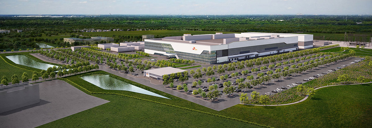
Bird’s-eye rendering of the completed plant. Provided by SK hynix
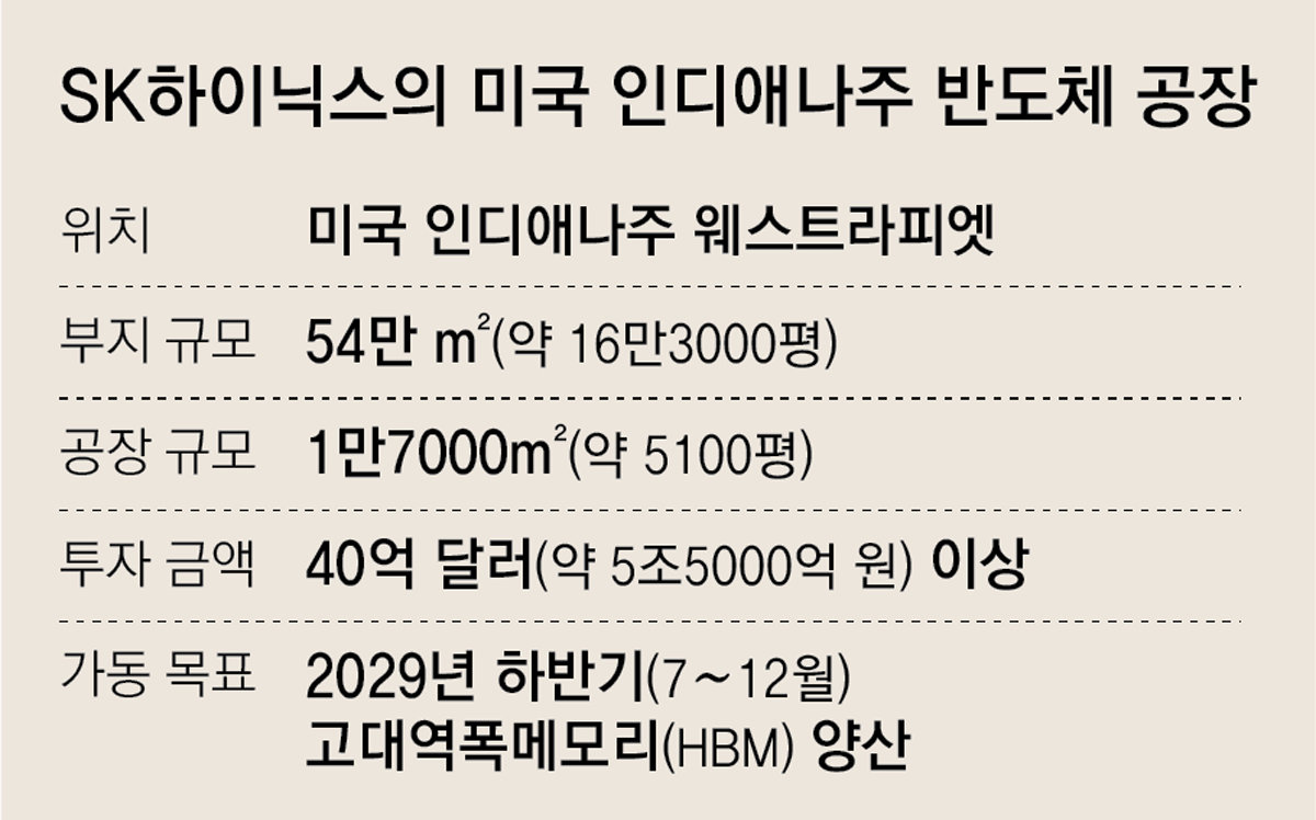
At the construction site, four ultra-large tower cranes, excavators, dump trucks, and special equipment such as gas-removal scrubbers required for the cleanroom were lined up. Land the size of about 75 soccer fields (540,000 ㎡, or approximately 163,000 pyeong), where the area’s main crop, corn, used to grow in neat rows, is being transformed into a cutting-edge HBM semiconductor production base.
● Base for “Made in USA” HBM On the 27th, SK hynix held a groundbreaking ceremony for its HBM advanced packaging production base at Purdue University’s Holloway Gymnasium in West Lafayette. Advanced packaging refers to the back-end process of stacking DRAM vertically and completing it as HBM.
SK hynix President and CEO Kwak Noh-jung, who attended the ceremony, emphasized that “the Indiana fab will serve as the first base to supply customers with ‘Made in USA HBM’ and as a foundation for strengthening the U.S. semiconductor supply chain while contributing to economic and national security.” Indiana Governor Mike Braun, Indiana Senator Todd Young, and Korean Ambassador to the United States Kang Kyung-wha were among the dignitaries from both countries in attendance.
More than USD 4.0 billion (about KRW 5.5 trillion) will be invested in the plant, which is scheduled to complete its cleanroom around October 2028. The company aims to begin mass production of next-generation HBM in the second half of 2029 (July–December).
Around 1,000 employees are expected to work at the site. In addition, the project is expected to create more than 7,000 direct and indirect jobs. About 100 partner companies in materials, components, and equipment are in discussions with SK hynix about entering the local market.
The Indiana fab will import cutting-edge DRAM wafers produced in Korea to Indiana, complete the stacking process there, and then conduct testing before final delivery to U.S. customers. “Based on wafer input, the facility is expected to secure annual production capacity of several hundred thousand HBM units,” CEO Kwak said.
Currently, 300 workers per day are being deployed for the on-site groundworks. When full-scale electrical and facility construction begins next year, more than 3,000 workers a day are expected to be mobilized. Kim stressed, “The site is equipped with state-of-the-art toilets, rest-area bunkers, and other facilities to provide maximum consideration for the workforce.” He added, “To prevent potential noise and dust damage to nearby residents, noise-reduction barriers have been voluntarily installed even though there are no relevant regulatory requirements.”
● Industry-academia cooperation with Purdue University – preferential hiring of former U.S. Forces Korea personnel On the same day, SK hynix also signed a memorandum of understanding with Purdue University, a prestigious local institution particularly strong in science and engineering, for research and development cooperation in advanced packaging. The company plans to conduct joint research with Purdue’s outstanding semiconductor-related talent, supported by an industrial-grade cleanroom that is rare for a university, and to cooperate on future recruitment.
Inside the cleanroom at Purdue’s Birck Nanotechnology Center, visited on the 26th, students in white cleanroom suits were busily conducting research. “Purdue operates state-of-the-art cleanrooms and a digital twin system so that researchers can train in an environment similar to actual industrial sites,” said Center Director Chen Zhihong, who provided the tour. “Deep ultraviolet (DUV) lithography equipment is also scheduled to be introduced within a few months,” he added.
He further noted, “SK hynix will need a broad spectrum of personnel ranging from undergraduate engineering majors to graduate researchers. The company will hire hundreds of employees over the next several years, and our goal is to train about 150 students at this center by 2028.”
To honor Indiana’s historical ties with Korea, having deployed about 140,000 troops during the Korean War, SK hynix will also operate a program giving hiring preference for fab-related positions to veterans who served with U.S. Forces Korea. The company announced that it plans to participate as an employer in the “Job Platform for Discharged U.S. Forces Korea Service Members,” operated by the Korea Chamber of Commerce and Industry and the Korea-U.S. Alliance Foundation.
ⓒ dongA.com. All rights reserved. Reproduction, redistribution, or use for AI training prohibited.
Popular News