Proposed industrial complex plan change with 490% floor area ratio
Maximizing production capacity amid memory boom
Strategic move to shift from double to triple-deck fabs
SK hynix in Yongin also planning a triple-fab complex
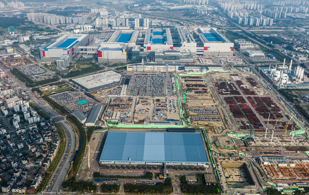
Samsung Electronics Pyeongtaek Campus P5 construction site. Provided by Samsung Electronics
Samsung Electronics will expand and build the core facilities of its semiconductor complex in Pyeongtaek, Gyeonggi Province, the “P5 Plants 1 and 2 (Fab 5 and 6),” by upgrading them from the existing “double fab (two-layer)” to a “triple fab (three-layer)” structure. This is a strategic move to maximize production capacity in line with the global “supercycle” in artificial intelligence (AI) semiconductors and memory. Not only Samsung Electronics but also SK hynix is planning all new fabs in the Yongin Semiconductor Cluster as triple fabs, leading to a rapid shift in domestic semiconductor fabs from double-fab to triple-fab structures.
According to the semiconductor industry on the 19th, Samsung Electronics recently submitted a “Samsung Electronics Industrial Complex Plan Amendment” that significantly raises the floor area ratio for building P5 Plants 1 and 2 in Pyeongtaek as triple fabs, from the previous 350% to up to 490%. This industrial complex plan change will be finalized after review by the Governor of Gyeonggi Province and approval by the Industrial Location Policy Deliberation Committee of the Ministry of Land, Infrastructure and Transport.
Earlier, at the beginning of 2023, the government eased regulations by revising the Enforcement Decree of the National Land Planning and Utilization Act to increase the floor area ratio cap in general industrial zones within national high-tech strategic industry complexes such as semiconductors, from the existing 350% to up to 490%, which is 1.4 times the statutory upper limit.
Pyeongtaek P5 Plants 1 and 2 are the world’s largest semiconductor plant on a single-fab basis. Construction began in 2022 and is underway with a target of final completion in 2030; at peak construction periods, up to 50,000 workers have been deployed on site. The facilities are scheduled to produce a wide range of products, including high-bandwidth memory (HBM), cutting-edge high-spec DRAM, next-generation V-NAND flash, and advanced foundry (contract semiconductor manufacturing) volumes.
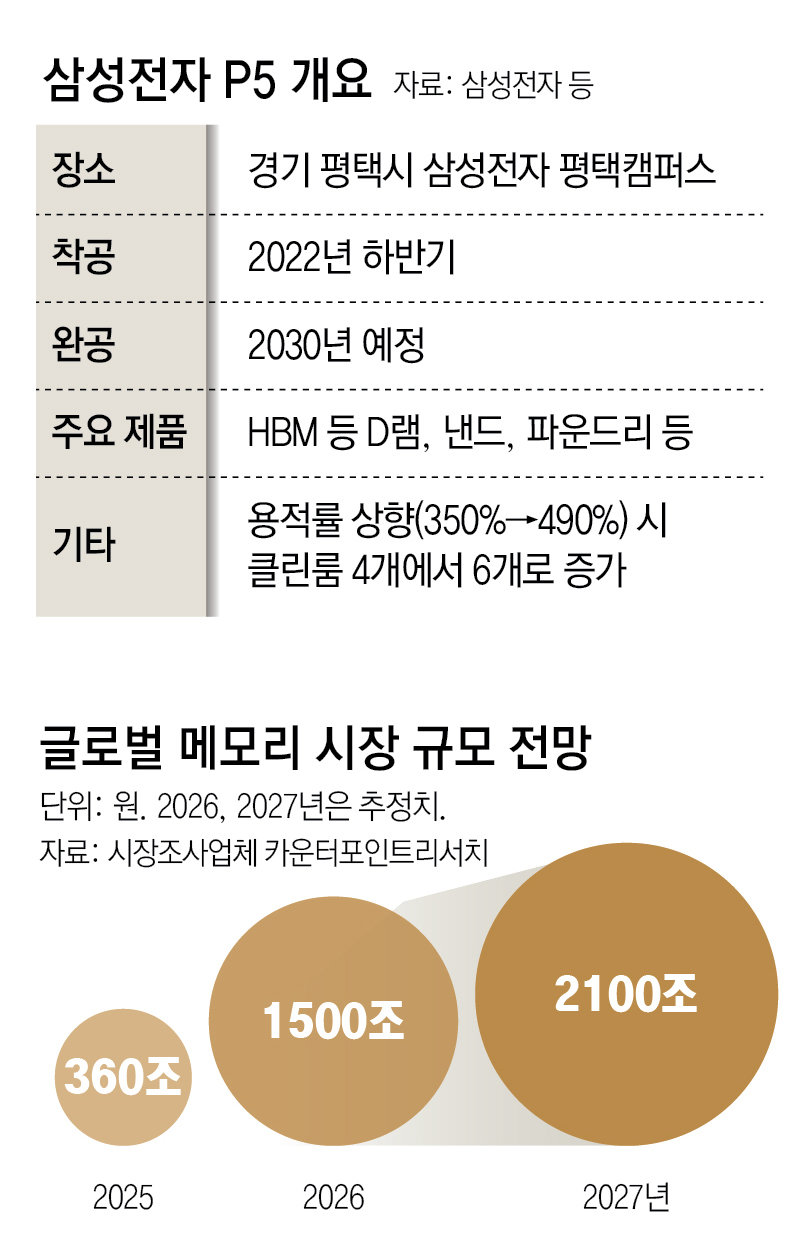
Up to P4 at the Samsung Electronics Pyeongtaek Campus, which recently began operations, each building followed a double-fab structure, accommodating four clean rooms. If the latest amendment is approved, P5 and beyond will be built as triple fabs, accommodating up to six clean rooms. As the number of clean rooms alone increases by 1.5 times, production capacity will also jump by more than 1.5 times. New semiconductor fabs to be built in both the national and general industrial complexes in Yongin by Samsung Electronics and SK hynix are likewise expected to adopt this triple-fab structure.
The backdrop to companies scaling up their semiconductor plants into triple fabs is the explosive growth of the global AI market. According to market research firm Counterpoint Research, the global memory market, estimated at about KRW 360 trillion last year, is forecast to expand to KRW 1,500 trillion this year and KRW 2,100 trillion next year. The boom in AI data center construction has triggered a surge in demand for HBM and high-capacity memory used in these facilities, creating a situation where securing supply volumes as quickly as possible has become imperative.
In a context where expansion of new power grids, securing water resources, and acquiring land have become extremely difficult, the triple fab is also the best alternative to overcome the physical constraints of limited space. It is also highly significant in that it maximizes the use of an already established “semiconductor ecosystem,” where hundreds of partner companies are clustered. SK Group Chairman Chey Tae-won recently emphasized the importance of expanding and concentrating existing semiconductor ecosystems in an interview with US media, stating, “Behind a large memory fab, there are 600 to 700 partner companies supplying materials, chemicals, and services,” and, “Only when power, water, and land can be secured and the related ecosystem moved together can fabs be built anywhere in the world.”
ⓒ dongA.com. All rights reserved. Reproduction, redistribution, or use for AI training prohibited.
Popular News