Samsung weighs expanding packaging hubs beyond South Chungcheong… “Nothing has been finalized”
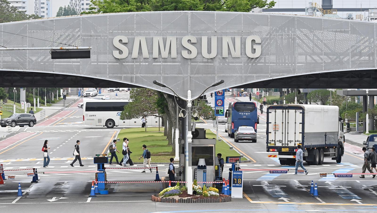
Samsung Electronics’ Suwon headquarters in Yeongtong-gu, Suwon-si, Gyeonggi-do. 2026.05.27 [Suwon=Newsis]
Samsung Electronics is pushing to build a semiconductor production base in Gwangju. This move is seen as both a response to the government’s policy line of revitalizing investment outside the Seoul metropolitan area and a strategy to strengthen competitiveness in advanced back-end processing (packaging) amid a surge in demand for artificial intelligence (AI) semiconductors.
According to business circles on the 9th, Samsung Electronics is reviewing a plan to build a new semiconductor packaging plant in Gwangju. If the process of etching circuits onto semiconductor wafers is the front-end process, the process of assembling and producing them into final products such as high-bandwidth memory (HBM) is the back-end process known as packaging.
If Samsung Electronics actually establishes a packaging base in Gwangju, it would be the first time since 1991, when it built the Onyang Campus in Asan-si, South Chungcheong Province, that the company has created a related production base in Korea. Samsung Electronics currently operates packaging lines mainly in the Chungcheong region, including the Onyang and Cheonan campuses. However, regarding plans to build a new semiconductor back-end processing production base in Gwangju, Samsung Electronics stated on the day that “nothing has been decided.”
Samsung Electronics is expected to unveil specific regional investment plans as early as the end of this month at a meeting of major group heads to be chaired by President Lee Jae-myung at the Blue House. SK hynix is also reportedly reviewing semiconductor investment plans in the Jeolla Nam-do area. Samsung Electronics Chairman Lee Jae-yong, SK Group Chairman Chey Tae-won, and others are all expected to attend the meeting of conglomerate leaders.
SK also weighing semiconductor investment in South Jeolla… Meeting of conglomerate leaders at Blue House at the end of this month
Samsung pursuing semiconductor plant in Gwangju
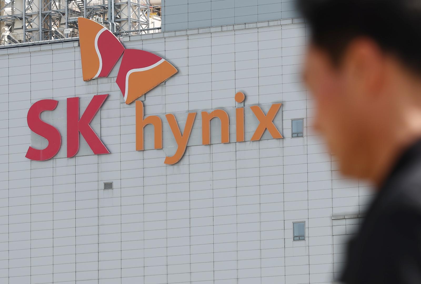
SK hynix headquarters in Icheon, Gyeonggi-do. 2026.4.23 ⓒ News1
Samsung Electronics’ push to build a new semiconductor packaging plant is seen as being driven by the growing importance of packaging, which finely connects semiconductors, as demand for high-performance memory such as HBM rises in line with the recent expansion of the AI market.
SK hynix is also reportedly reviewing the establishment of a semiconductor packaging production base in the Honam region, particularly in South Jeolla Province. However, SK hynix has already announced plans to invest KRW 19 trillion in building its advanced packaging plant P&T7 in Cheongju-si, North Chungcheong Province, and began construction this April. With Gyeonggi Yongin and North Chungcheong Cheongju as its semiconductor production hubs, the company is said to be considering ways to establish a back-end processing production base in the South Jeolla area that can be linked to these sites.
In the semiconductor industry, the fundamental reason cited for companies considering investment in regions outside the metropolitan area is “infrastructure security.” Existing semiconductor clusters in the Seoul metropolitan area, such as Yongin-si and Pyeongtaek-si in Gyeonggi-do, are said to be approaching their effective limits in supplying large-scale power and water. In contrast, non-metropolitan regions such as Honam have relatively abundant renewable energy production, including solar and wind power, as well as more ample water supply. Synergies with Hyundai Motor Group’s physical AI value chain project in Saemangeum, North Jeolla Province, where the group has decided to invest, are also seen as an advantage.
In addition, the government’s announced policy of actively supporting companies that invest outside the metropolitan area is cited as another reason for considering the construction of semiconductor production bases in Honam. At a press conference marking his first year in office on the 8th, President Lee Jae-myung said, “We are asking companies, if possible, to invest in regional areas.” He also emphasized, “We will soon present to the public large-scale investment projects that will bring about a major shift in our growth strategy.”
However, both Samsung Electronics and SK hynix are reportedly reluctant to relocate front-end semiconductor processes to the Honam region. Samsung Electronics is said to have reviewed a plan to disperse some of the front-end semiconductor production lines (fabs) that were initially to be built in the Yongin Semiconductor National Industrial Complex to Honam, but ultimately judged this difficult due to efficiency issues.
Front-end semiconductor processing requires the creation of an ecosystem in which hundreds of materials, parts, and equipment companies are clustered. The argument is that artificially splitting the existing supply chain in the Seoul metropolitan area would inevitably increase logistics costs and reduce process efficiency.
ⓒ dongA.com. All rights reserved. Reproduction, redistribution, or use for AI training prohibited.
Popular News