Originally slated for Q3, supply moved up significantly
Speed improved by 20%, energy efficiency by 16%
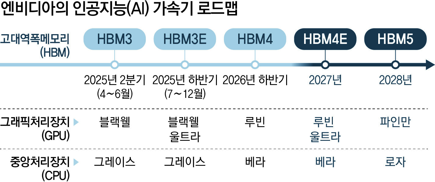
To feature NVIDIA AI accelerators
Samsung Electronics becomes first in Korea to reach KRW 2,000 trillion in market capitalization
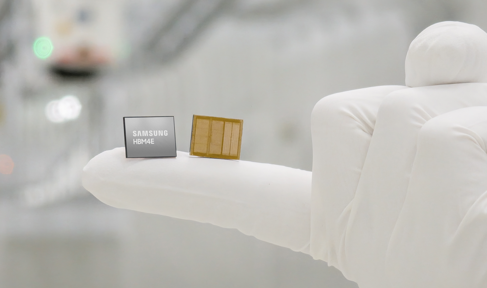
On the 29th, Samsung Electronics unveiled the actual product of its 7th-generation high bandwidth memory (HBM), “HBM4E,” which it has supplied to global customers. The fingertip-sized HBM is produced by stacking DRAM chips manufactured with ultra-fine processes. HBM4E is expected to be mounted on Nvidia’s next-generation artificial intelligence (AI) accelerator “Vera Rubin Ultra,” slated for launch next year. Source: Samsung Electronics
● Samsung supplies world’s first ‘HBM4E sample’
On the 29th, Samsung Electronics supplied 12‑high samples of “HBM4E,” its 7th‑generation high bandwidth memory (HBM), to global customers for the first time in the world. This moved up the supply schedule, which had initially been expected for the third quarter (July–September) of this year. Having become the first company in the world to mass-produce and ship HBM4 (6th generation) in February, Samsung has been capturing “world-first” titles in the artificial intelligence (AI) memory segment this year. With Samsung’s early sample supply, market observers expect SK hynix and Micron to also accelerate their development timelines.
Samsung Electronics announced on the 29th that it has supplied 12‑high samples of its 7th‑generation high bandwidth memory (HBM) “HBM4E” to global customers for the first time in the world. This comes just three months after it became the first company globally to mass-produce and ship HBM4, the 6th generation. Analysts say Samsung has shaken off its underperformance up to the 5th generation and fully regained leadership in AI memory chips.
● ‘Ultra gap’ via memory–foundry collaboration
Samsung Electronics stated that it shipped HBM4E 12‑high samples to global customers on the same day. The samples are reported to have been supplied to big tech companies, including Nvidia, that mount HBM on their AI chips.
HBM4E is a high-performance memory to be applied to Nvidia’s AI accelerator “Vera Rubin Ultra,” which is scheduled for release in 2027. Samsung Electronics has already become the first company in the world to mass-produce and ship HBM4 for Nvidia’s “Vera Rubin,” due for launch in the second half of this year (July–December). Starting with this sample supply, Samsung plans to pursue mass production of HBM4E after performance verification and optimization processes with customers.
For semiconductor companies, sample supply is a signal that development has entered its final stage. In particular, as the generational replacement cycle for Nvidia-led AI accelerators becomes extremely short, the speed of HBM sample supply is effectively regarded as order-winning competitiveness.
The semiconductor industry is also focusing on the unusually early timing of this sample supply. This is because it has been moved up significantly from the third quarter (July–September), which Samsung had indicated in March this year as the sample supply window. Accordingly, some analysts say the mass-production schedule, previously expected around the end of this year, may also be brought forward. Because HBM requires a long optimization period in which the product is repeatedly verified and refined with customers, the sample supply timing inevitably affects the subsequent mass-production schedule.
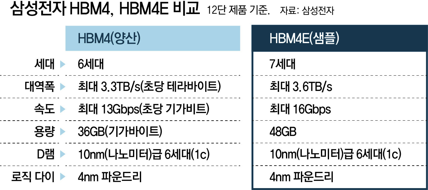
The unusually rapid development of 7th‑generation HBM is also being attributed to collaboration between Samsung’s memory and foundry (contract manufacturing) divisions. Samsung’s HBM4E is produced by stacking DRAM fabricated using a 10‑nanometer (nm, one nanometer is one-billionth of a meter)‑class 6th‑generation ultra-fine process (1c). The “logic die” that connects the DRAM and the graphics processing unit (GPU) and serves as the “brain” of the HBM uses the foundry’s 4nm process. Unlike its competitors, which must collaborate with Taiwan’s TSMC, Samsung can leverage its own foundry, enabling faster optimization.
The new HBM4E also improves performance, efficiency, and capacity over its predecessor. Samsung explained that HBM4E supports speeds of up to 16 Gbps (gigabits per second) per pin. This means it can transfer up to 16 Gb of data per second, more than a 20% improvement over HBM4. Bandwidth, which represents the volume of data processed per second, has also increased by 0.3 TB (terabytes) per second compared with the previous generation. At the same time, energy efficiency has improved by 16% over its predecessor, and capacity has expanded to 48 GB (gigabytes) for the 12‑high configuration. Samsung added, “Depending on customer demand, the product lineup can be expanded to 8‑high (32 GB) and 16‑high (64 GB).”
● HBM speed race pushes Samsung market cap above KRW 2,000 trillion
Samsung’s early sample supply is expected to accelerate competitors’ development schedules as well. SK hynix stated during its first-quarter (January–March) earnings announcement that it “plans to begin sample supply (of HBM4E) in the second half of the year” and that “development is progressing smoothly with a target of mass production next year (2027).” Micron’s Manish Bhatia, Executive Vice President of Global Operations, said at a JPMorgan conference on the 20th (local time), “HBM4E development is progressing smoothly, and we expect a ramp-up in 2027.”
Meanwhile, Samsung Electronics’ share price closed at KRW 317,000 on the day, up 5.84% from the previous trading session, on news of the HBM4E sample supply. Including preferred shares, Samsung’s total market capitalization reached KRW 2,016 trillion at the close, making it the first domestically listed company to surpass KRW 2,000 trillion in market value. Supported by net institutional buying, the KOSPI closed at 8,476.15, up 290.86 points (3.55%) from the previous session, marking an all-time closing high.
ⓒ dongA.com. All rights reserved. Reproduction, redistribution, or use for AI training prohibited.
Popular News