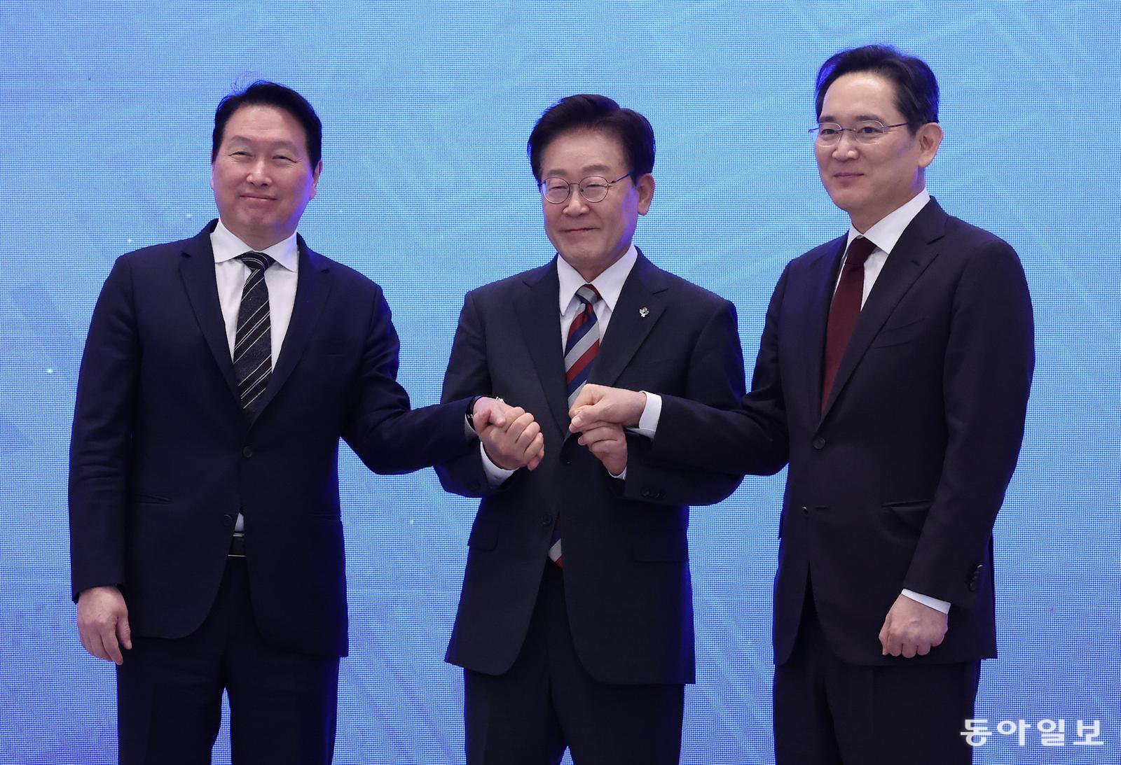
On the 29th at the Blue House during the “Korea’s Great Leap Forward: Three Mega Projects National Briefing,” President Lee Jae-myung is seen joining hands with Samsung Electronics Chairman Lee Jae-yong (right) and SK Group Chairman Chey Tae-won. President Lee stated, “I would like to call Chairman Lee and Chairman Chey national heroes, heroes of the people,” adding, “I will shake hands once to signify our firm intention to carry out this plan without a hitch going forward.” Photo by Kim Jae-myung base@donga.com
At the “Korea’s Great Leap Forward: Three Mega Projects National Briefing” held at the Blue House on the 29th, plans to build four front-end semiconductor fabs (manufacturing plants) in Gwangju by Samsung Electronics and SK hynix were officially announced. Excluding existing capital-area clusters such as Yongin, the volume of new semiconductor funds to be injected into non-capital regions such as Gwangju and the Chungcheong area alone will reach approximately KRW 1,000 trillion.
● KRW 800 trillion to be invested in new Gwangju semiconductor plants
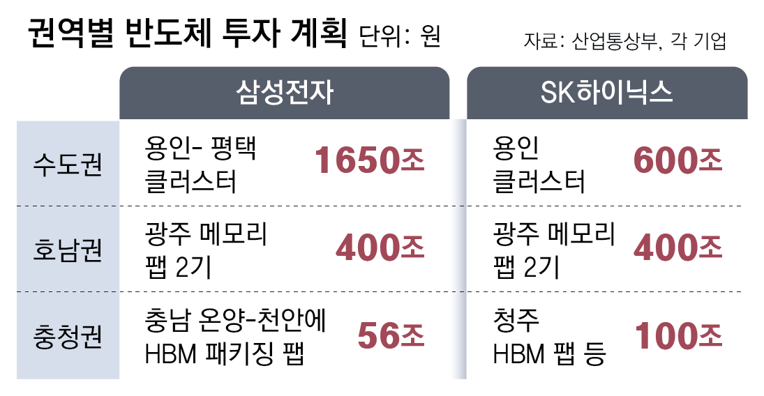
The core of this investment plan is securing Gwangju as a new semiconductor hub. Samsung Electronics and SK hynix will each invest KRW 400 trillion, for a total of KRW 800 trillion, in Jeonnam-Gwangju Integrated Special City to establish four state-of-the-art front-end memory fabs (two each). This involves front-end fabs, the core of semiconductor manufacturing in which wafers are loaded and circuits are etched, rather than back-end processes (packaging) involving materials and components or final product finishing. It is the first time in Korea that large-scale front-end fabs are being newly built in a non-capital region.
At the national briefing, the leaders of Samsung and SK stressed the necessity of expanding semiconductor investment. Samsung Electronics Chairman Lee Jae-yong explained the background of the Gwangju fab investment, saying, “Due to artificial intelligence (AI), technological paradigms are changing at a pace beyond imagination, and the market assessment is that even active (semiconductor) investment is insufficient to meet demand.”
SK Group Chairman Chey Tae-won likewise stated, “Even if we carry out early investments of KRW 600 trillion in Yongin, Gyeonggi Province, and KRW 100 trillion in Cheongju, North Chungcheong Province, to increase memory production, supply shortages will continue in the future,” adding, “We will invest approximately KRW 400 trillion in the southwest region to create new fabs.”
The specific sites of the Gwangju semiconductor plants are expected to be unveiled at the “Honam Region Advanced Industry Investment Plan Briefing” to be held on the 30th at Kimdaejung Convention Center in Seo District, Gwangju. In the region, there is speculation that Samsung Electronics may build a new plant at the Gwangju military airport site, while SK hynix may construct a plant in Advanced District 3 spanning Gwangju and Jangseong in South Jeolla Province. Regarding the completion timeline, Presidential Chief of Staff Kang Hoon-sik indicated 2030, within the term of the Lee Jae-myung administration.
However, some observers believe it will be difficult to meet the cluster completion schedule within the current administration as presented by the government. This is because it will take time to establish power and water infrastructure and to secure extreme ultraviolet (EUV) lithography equipment. Samsung Electronics has disclosed 2040 as the investment horizon for this project.
Within the semiconductor industry, there is an assessment that the so-called “semiconductor southern limit line (southern Gyeonggi Province),” long considered difficult to cross due to infrastructure issues, has now been broken. Chief of Staff Kang said, “With this investment, the so-called semiconductor southern limit line has collapsed, and it has been proven that large-scale advanced industries are possible in provincial regions as well.” He added, “Samsung Electronics’ semiconductor profits over the past 40 years totaled KRW 295 trillion, yet this year’s profit alone is KRW 350 trillion,” and went on to say, “Criticism by some opposition parties that this is being done by ‘twisting their arm’ completely ignores corporate realities.”
● Semiconductor belt linking the capital, Chungcheong, and Honam regions
On this day, investment amounts by semiconductor base were also specified. The plan is to build a “K-Memory” production belt connecting the capital area, Chungcheong, and Honam.
Samsung Electronics will invest KRW 56 trillion in back-end processes in the Chungcheong region, including Onyang and Cheonan, and KRW 1,650 trillion in the capital area, including Pyeongtaek and Yongin, where it has plans to build or expand existing fabs. Including the Gwangju investment, the company plans to execute a total of KRW 2,106 trillion in semiconductor investments by 2040. SK hynix will also proceed with semiconductor investments totaling KRW 1,100 trillion, including KRW 100 trillion in its Cheongju packaging hub and KRW 600 trillion in the Yongin semiconductor cluster.
The background to the two companies’ plan to undertake massive semiconductor investments totaling KRW 3,206 trillion, including KRW 956 trillion in non-capital regions, lies in the surge in memory demand driven by the spread of AI and the saturation of infrastructure in the capital area. According to market research firm Omdia, the global memory market is projected to grow fourfold within five years, from USD 200 billion (about KRW 309 trillion) in 2025 to USD 800 billion (about KRW 1,236 trillion) in 2030.
Through expanded investment, the operational timelines of existing capital-area production bases will also be accelerated. Based on final fab construction, completion of the Samsung Yongin National Industrial Complex will be moved up from 2042 to 2035, and the SK Yongin General Industrial Complex from 2045 to 2033, advancing the schedules by seven and 12 years, respectively. Construction of Samsung’s Pyeongtaek Lines 5 and 6 will be converted to simultaneous build-out, shortening the overall timeline by three to four years and doubling national memory production capacity within five years. The Yeongnam region will be developed as a “semiconductor materials, parts, and equipment innovation hub.”
Kwon Seok-jun, professor in the Department of Chemical Engineering at Sungkyunkwan University, said, “At a time when it is urgent to expand production facilities in line with changes in the AI industry, the establishment of a large-scale regional investment plan is a positive development,” and added, “Since companies have decided on massive investments, the government must prepare robust support measures to reduce management uncertainty.”
ⓒ dongA.com. All rights reserved. Reproduction, redistribution, or use for AI training prohibited.
Popular News