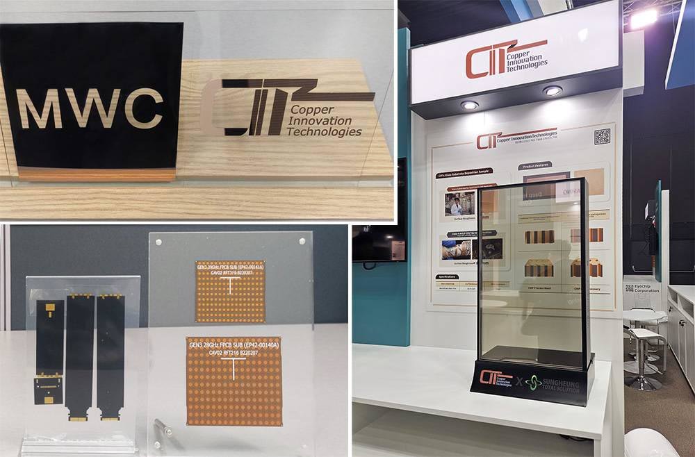
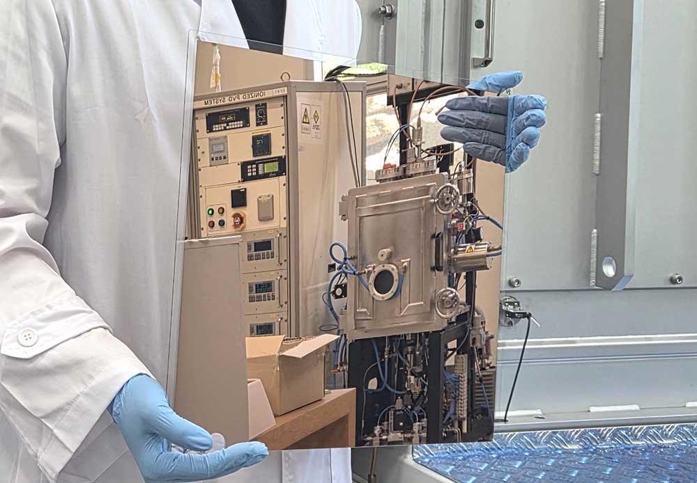
Copper Innovation Technologies (CIT), a materials technology startup, has unveiled the 'CuFlat-PKGCore', a semiconductor packaging board for AI accelerators, based on its independently developed ASE (Atomic Sputtering Epitaxy) deposition technology.
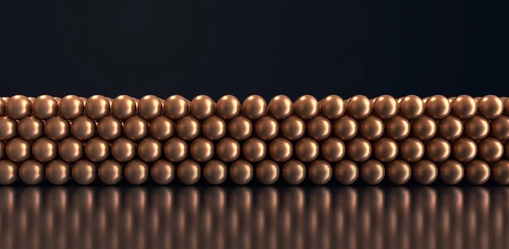
The CuFlat-PKGCore is a product that deposits copper on a glass substrate, which is the next-generation semiconductor package substrate material. It enhances design flexibility by depositing copper smoothly and uniformly, replacing complex chemical processes with a single deposition process, thereby improving production speed and efficiency. It also minimizes chemical wastewater and carbon emissions during manufacturing. When applied to data centers, it is expected to reduce power and cooling water consumption by half.
CIT plans to challenge for the CES 2026 Innovation Award with the CuFlat-PKGCore and to actively enter the global semiconductor packaging market.
var WiderPlanetAdRendererVar = {
type : "script",
passback : '/images/common/pc_view_banner.jpg',
category : "pc_view_banner",
width : "468",
height : "60",
zoneid : "30713",
targetid : "kb_pc_view_ad"
};
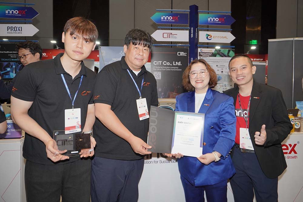
CIT is also building global partnerships. It is currently testing product supply with AGC, a Japanese glass substrate and transparent antenna manufacturing company, and a U.S. semiconductor equipment company. Additionally, it is jointly developing AI accelerator substrates with a domestic conglomerate to enter the global market. Furthermore, it is expanding the applicability of ASE deposition technology through collaborations with various companies.
IT Donga Reporter Han Man-hyuk (mh@itdonga.com)
AI-translated with ChatGPT. Provided as is; original Korean text prevails.
ⓒ dongA.com. All rights reserved. Reproduction, redistribution, or use for AI training prohibited.