Seoul National University of Science and Technology (SEOULTECH) Technology Holdings is enhancing the commercialization of its subsidiaries’ technologies and their market competitiveness through the BRIDGE 3.0 program. ITDongA introduces the technological capabilities, commercialization achievements, and entrepreneurial spirit of Technology Holdings’ subsidiary companies that are growing with such support.
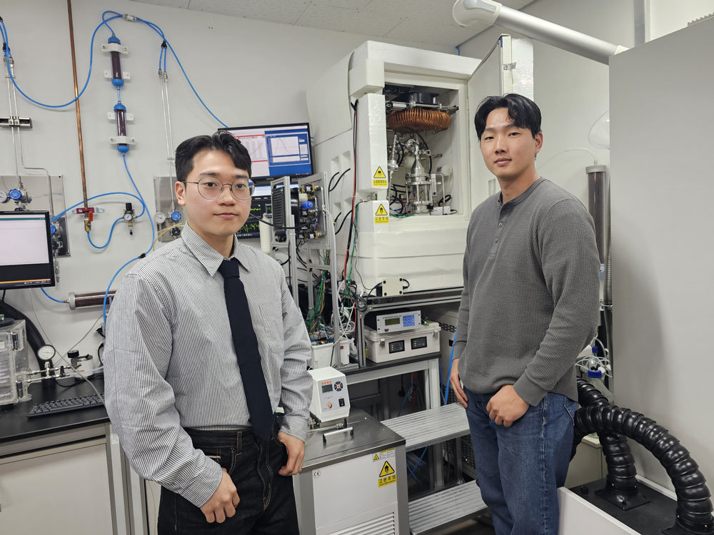
K-Nano PM Ji Hyoung-woo (left) and researcher Lee Yoo-seon (right) / Source = ITDongA
As semiconductor processes have become finer at the nanometer (nm, one-billionth of a meter) scale, it has become essential to capture particles at this minuscule level to secure a competitive semiconductor yield. A startup has developed an innovative monitoring system in pursuit of a defect-free semiconductor manufacturing process. That company is K-Nano (CEO Kwak Dong-bin), a subsidiary of SEOULTECH Technology Holdings.
Technology-focused startups often draw attention to the CEO’s vision, but the real driving force behind corporate growth is the effort of researchers who turn that vision into technology in the field. ITDongA spoke with Project Manager (PM) Ji Hyoung-woo and hardware engineer Lee Yoo-seon, who are at the forefront of K-Nano’s technological innovation, about the future of semiconductor process monitoring. The Bridge 3.0 project run by SEOULTECH Technology Holdings is part of the Ministry of Education’s “University Creative Assets Practical Utilization Support Project,” which aims to connect university research achievements with companies to facilitate technology transfer and commercialization.
- Please introduce yourselves. How did you come to join K-Nano?PM Ji Hyoung-woo: I majored in Mechanical System Design Engineering at SEOULTECH and then worked for about a year as an AI software developer. I have experience in both hardware and software, and it was researcher Lee Yoo-seon, who joined first and recommended me as a good fit, that led me here. When I first met CEO Kwak Dong-bin, I saw that he was not simply looking for more hands but was determined to pioneer a new path not yet seen in Korea, backed by a clear goal and confident leadership. That convinced me to join.
Researcher Lee Yoo-seon: I also graduated from the Department of Mechanical Engineering at SEOULTECH and became connected with CEO Kwak while preparing for my master’s and doctoral studies. As an early member of his lab, I carried out research projects on air filtration. Experiencing the entire R&D (research and development) process—from precisely analyzing on-site problems to deriving practical solutions—gave me confidence in this role. I was drawn to the tangible growth of seeing theory implemented as real industrial technology, and naturally became one of the founding members.
- What technologies is K-Nano developing, and what are your specific roles?PM Ji Hyoung-woo: K-Nano develops equipment that analyzes fine particles in advanced industries. In our current core area, semiconductor processes, even a single tiny, invisible particle can be a major cause of yield decline, and our mission is to monitor such particles in real time. As PM, I coordinate the entire process from product planning to development and oversee the development roadmap that creates synergy between the hardware and software teams. We are concentrating all our efforts on completing K-Nano’s first commercial product, which is scheduled for release this year.
Researcher Lee Yoo-seon: As a hardware engineer, I am responsible for the design and construction of equipment and automation systems. My main tasks include verifying our technology at the lab scale and designing the hardware architecture so it can actually be set up in semiconductor production sites. I focus on advancing the system so that sensors, actuators, and control units are organically integrated to secure data reproducibility even during repeated experiments.
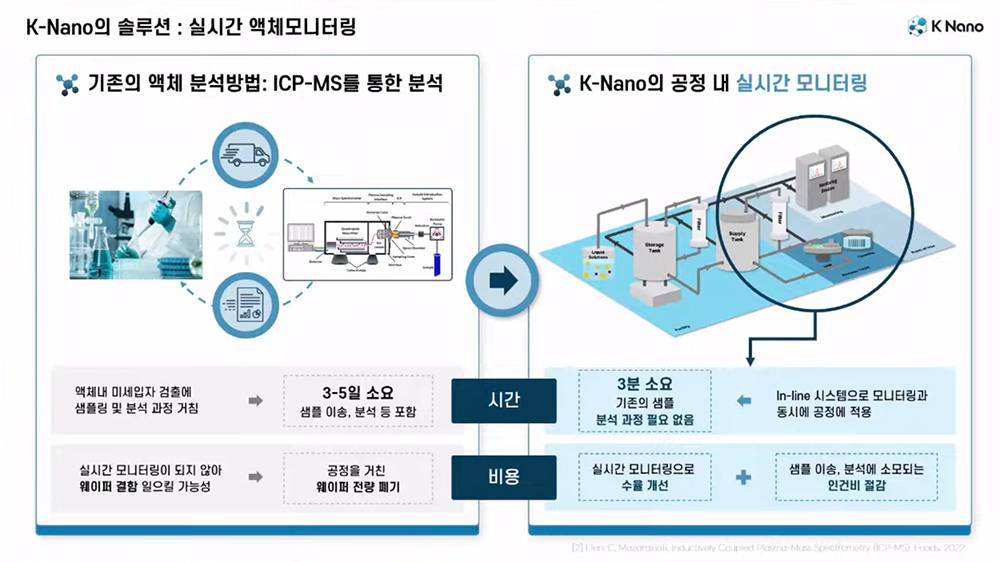
Explanation of the differences between ICP-MS-based analysis and K-Nano’s real-time monitoring / Source = K-Nano
- What differentiates K-Nano’s monitoring system from others?Researcher Lee Yoo-seon: Existing optical liquid particle counters (LPCs) have clear limitations in measuring ultra-fine particles smaller than 20 nm. They also frequently mistake bubbles in the solution for actual particles, which lowers data reliability. We chose a method that converts particles in liquid form into aerosols and then measures their concentration by particle size.
PM Ji Hyoung-woo: As a result, we have established a foundation to analyze fine particles at around 10 nm in real time, which was difficult to capture with existing technologies. Our core asset lies in our aerosol conversion technology and know-how, which sprays liquid into the air so it can be analyzed with SMPS (Scanning Mobility Particle Sizer), a fine dust analysis technology. We have also enhanced data precision. Data obtained from the equipment often include not only particle information but also NVR (Non-Volatile Residue), such as non-volatile organic matter, which is mixed in and causes confusion in analysis. We developed a solution using AI machine-learning algorithms that precisely separates and analyzes actual particles and residues. This is a proprietary technology for which we have applied for patents in Korea and the United States.
- How has the semiconductor industry responded in practice?
PM Ji Hyoung-woo: Through a PoC (Proof of Concept, a stage where performance is verified before new technology adoption) project with Samsung Electronics, we directly analyzed samples of CMP (Chemical Mechanical Polishing, a process for planarizing semiconductor wafer surfaces) slurry, which is a polishing material, to prove the on-site feasibility of our technology. When tested alongside competing products, we were evaluated as having a far superior ability to detect nanoparticles. At the Innovation Leaders Summit (ILS) in Japan last December, we felt the potential for business expansion firsthand as inquiries about precision nanoparticle analysis technology poured in immediately after opening our booth, not only from the semiconductor sector but also from a range of industries including secondary batteries, fine chemicals, and biotech.
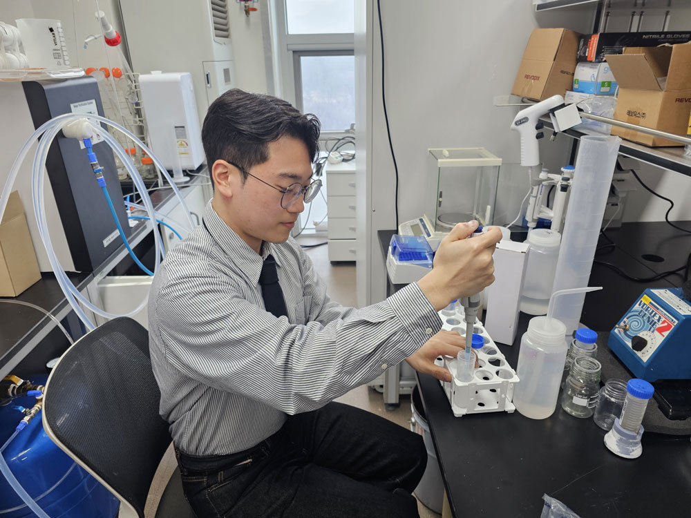
K-Nano PM Ji Hyoung-woo conducting tests / Source = ITDongA
- The roles of other team members working hard alongside you also seem important.PM Ji Hyoung-woo: Application engineer researcher Cho Sung-min and software (S/W) engineer Lee Seung-woo are our key pillars. Researcher Cho has led the project with Samsung Electronics, advancing our data algorithms and achieving outcomes such as academic paper publication and patent applications. Researcher Lee has carried out complex fluid analysis simulations to derive optimal mechanical designs and implemented them as user-friendly control software, thereby improving overall system completeness.
Researcher Lee Yoo-seon: Researcher Cho has outstanding communication skills—something often lacking in technology-focused startups—which is a big asset in meetings with overseas companies or partner firms. As our respective areas of expertise differ, there were initial communication barriers due to terminology gaps, but we worked to align our understanding by visualizing and sharing drawings and data simulation materials.
- Have there been difficulties as a young company? What is the internal atmosphere like?PM Ji Hyoung-woo: As PM, I was initially busy just trying to understand the system, and I also had a personal fear of public speaking. However, right after I joined, the CEO entrusted me with an important IR (Investor Relations) presentation. To live up to that trust, I studied thoroughly, to the point of memorizing the entire slide order and script, and in the process I deepened my understanding of the system and overcame my fear of presentations. Our team has strong bonds; we even work out at the gym or go running together outside of work. The CEO’s passionate example, constantly working in the field harder than anyone else, is a major source of motivation for the entire team.
Researcher Lee Yoo-seon: Technically, minimizing particle loss during the sampling process has been a major challenge. To address this, we repeatedly improved the hardware by simplifying the flow path structure and minimizing dead volume (unnecessary space). The internal culture is very horizontal. As there is not a large age gap with the CEO, it is easy to voice opinions and engage in technical discussions, and communication is based more on roles and responsibilities than on titles. This flexibility is the driving force behind rapid decision-making and technological challenges.
- How helpful has the support program from SEOULTECH Technology Holdings been?PM Ji Hyoung-woo: Since the company was only established last September and is barely five months old, we lacked information. Technology Holdings swiftly updated us on commercialization projects and events that early-stage startups can apply for. Through seminars, it also created networking opportunities with various companies and provided legal advisory support, thanks to which we were able to quickly obtain our venture business certification. They are a reliable supporter that is genuinely pleased, as if it were their own achievement, when we secure investment or generate sales results.
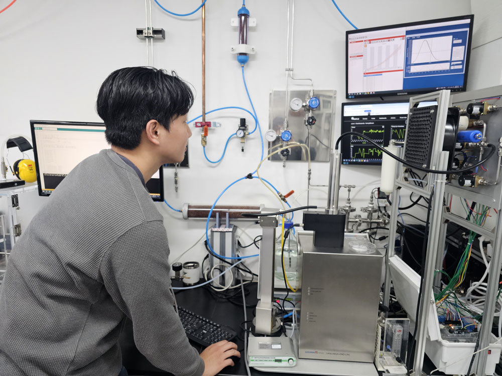
Researcher Lee Yoo-seon monitoring data / Source = ITDongA
- What are K-Nano’s future plans and ultimate aspirations?Researcher Lee Yoo-seon: We plan to expand beyond CMP slurry, which is currently undergoing PoC, to apply our technology to various semiconductor process liquids such as cleaning solutions and etchants. Furthermore, we aim to evolve into a quality management platform for entire processes by strengthening predictive diagnostics based on real-time data. Ultimately, K-Nano seeks to become a core infrastructure player in achieving defect-free operations not only in semiconductors but also across Korean industries such as biotech and fine chemicals.
PM Ji Hyoung-woo: We plan to launch our first product on the market this year together with our partner company ART+. Although we face many first-time difficulties as a young company, there is great satisfaction in running harder and learning more along the way. Our goal and desire is to make K-Nano a name that every engineer in the global industry recognizes in the field of nanoparticle detection.
Reporter Kim Young-woo, ITDongA (pengo@itdonga.com)
ⓒ dongA.com. All rights reserved. Reproduction, redistribution, or use for AI training prohibited.
Popular News