Intel is set to commence commercialization of its 18A (angstrom) process, equivalent to a 1.8-nanometer semiconductor process, four years after its announcement. On October 10, Intel revealed plans to disclose details of the next-generation consumer processor lineup, the 'Intel Core Ultra Series 3,' by the end of this year. This Core Ultra Series 3 will be manufactured using the 18A process at Intel's Fab 52 in Arizona.
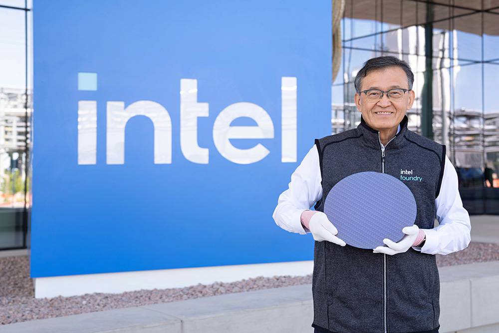
Intel CEO Lip-Bu Tan holding the first shipped 18A process wafer / Source=Intel
In 2021, Intel announced at the 'Intel Accelerate' event that it would begin mass production of the 20A process by 2025. However, due to deteriorating foundry profitability, successive restructuring, and a CEO change, Intel considered selling or separating its foundry business, leading to the abandonment of the 20A process. Nevertheless, with support from the U.S. government's 'CHIPS and Science Act' and equity acquisitions in 2024, Intel skipped the 20A and moved directly to the 18A process. The 18A process, below 2 nanometers, is considered more advanced than competitors Samsung Electronics and TSMC.
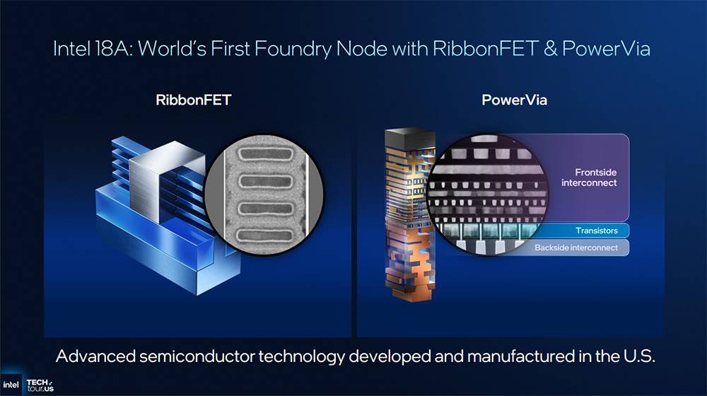
Intel's Comeback: Key Features of the 18A ProcessIntel's 18A process is the first sub-2-nanometer process developed in the United States, offering up to 15% better performance per watt and 30% higher chip density compared to the Intel 3 process. Starting with 18A, Intel replaced the FinFET transistor structure, used for over a decade, with RibbonFET. FinFET is a structure that allows control of the transistor gate on three sides, introduced by Intel under the name Tri-Gate since 2011.
The core of Intel's 18A process is the application of the new transistor structure 'RibbonFET' and the backside power delivery technology 'PowerVia' / Source=Intel
RibbonFET is Intel's term for the Gate-All-Around structure. Unlike FinFET, where the gate is on three sides, the ribbon-shaped gate surrounds almost all sides, providing higher integration and current control performance. Additionally, PowerVia, which places the semiconductor's power supply line on the back of the chip, was applied to reduce power loss and voltage drop.
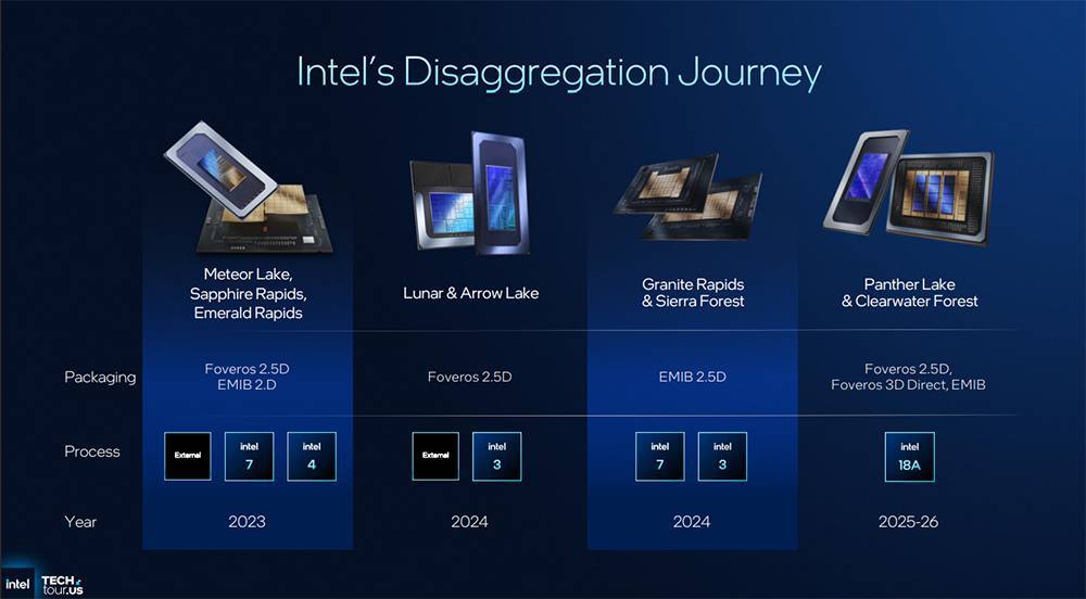
Following the Intel 3 process-based release in 2024, the Panther Lake and Clearwater Forest based on the 18A process will be launched by the end of this year / Source=Intel
Intel will produce the Core Ultra Series 3 for laptops and the Xeon 6+ server x86 processors using the 18A process. The Core Ultra Series 3 combines the efficiency of existing low-power CPUs with high-performance CPU capabilities, featuring up to 16 high-performance cores and 50% improved low-power cores. The graphics card includes up to 12 Xe cores, offering 50% improved performance over the previous generation, and provides AI processing performance of up to 180 TOPS (180 trillion operations per second).
The Xeon 6+, codenamed Clearwater Forest, is a server CPU with up to 288 efficiency cores. The x86 server market has traditionally competed with high-performance chips, but with the advent of the AI era, tasks requiring parallel processing for large-scale users have increased, leading to the introduction of the low-power core configuration of Clearwater Forest. The Clearwater Forest-based Xeon 6+ processor offers 17% improved instructions per cycle (IPC) performance over the previous generation and is scheduled for release in the first half of 2026.
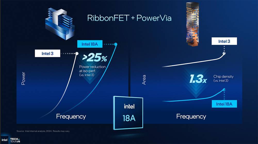
Intel announced that with the application of RibbonFET and PowerVia, power efficiency improved by up to 25% and chip density increased by 30% compared to Intel 3 / Source=Intel
Despite Intel's business foundation being shaken in recent years, the outlook is positive. In April last year, Intel announced Microsoft as the first major customer for the 18A process, and in September, NVIDIA announced a KRW 6.9 trillion investment in Intel to jointly manufacture CPU and GPU fusion products. Reports also emerged that competitor AMD is negotiating to use Intel's foundry for chip manufacturing. With the start of 18A mass production by the end of this year, Intel's crisis narrative is expected to gradually subside.
TSMC and Samsung Foundry in Pursuit with 2nm Competition
While Intel has taken the lead with the commencement of the 18A process, equivalent to 1.8 nanometers, TSMC and Samsung Foundry are not trailing far behind. As process nodes shrink, density and performance efficiency improve, but there are gaps in manufacturing costs and process maturity. TSMC will start the N2 process, equivalent to 2 nanometers, in the second half of this year, with the improved N2P process starting in the second half of 2026. In terms of performance, it is 18% faster with the same power consumption and reduces power consumption by up to 36%. Circuit density is 1.2 times higher, and chip density is 1.15 times higher than N3E.
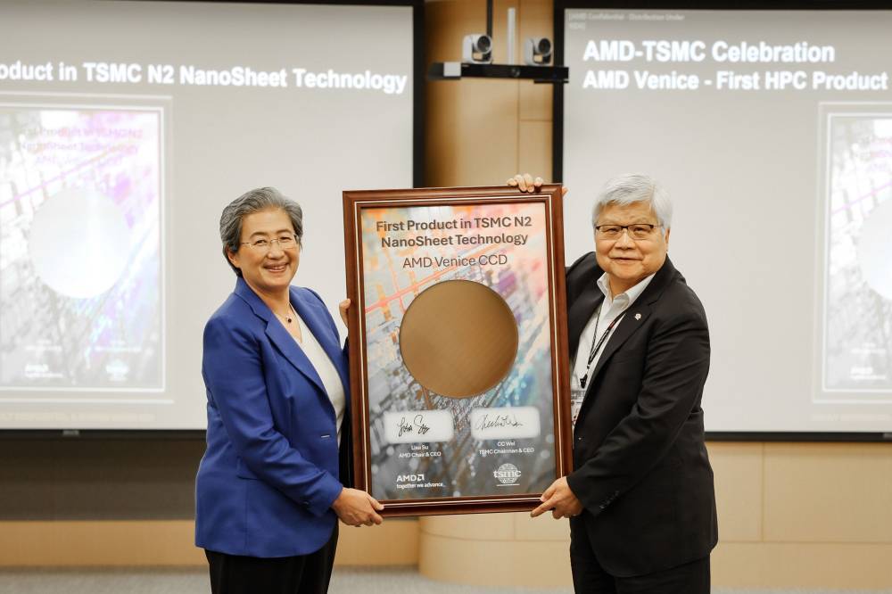
The first product of TSMC's N2 process is confirmed to be AMD's server CPU, AMD EPYC / Source=AMD
TSMC has begun construction of its third plant in the U.S. to produce N2, 1.6-nanometer process semiconductors, and on the 17th local time, began production of NVIDIA Blackwell chips using the N4P process, equivalent to 4 nanometers, at its Arizona plant. TSMC is allocating 30% of its high-performance semiconductor manufacturing capacity to the U.S. and is working to expand the foundry industry base.
Rebellion plans to design chips using Arm's total design and produce them at Samsung Foundry's 2nm process / Source=Arm
Samsung Foundry will also begin mass production of the second-generation 2-nanometer (SF2P) process, equivalent to 2 nanometers, by the end of this year. This chip offers 12% improved performance and 25% improved power consumption over the first generation, while reducing area by 8%. Samsung Foundry has already signed a KRW 22 trillion semiconductor foundry contract with Tesla last month. Domestic semiconductor company DeepX is collaborating with Samsung Foundry and Gaonchips to produce the DX-M2 semiconductor, and Rebellion is designing chiplet semiconductors with Arm and ADTechnology to be manufactured using the SF2P+ process.
Intensified Competition with Intel's Entry: Who Will Take the Market Share?According to market research firm TrendForce, TSMC held a 70.2% share of the global foundry market in the second quarter of 2025. Samsung Foundry's share was 7.3%, and China's SMIC held 5.1%. Despite the market being heavily tilted towards TSMC, Intel's entry into a more advanced process than TSMC has put TSMC and Samsung Foundry on alert. However, a finer process does not automatically guarantee competitiveness.
Intel's 18A, with its early adoption of PowerVia, is advantageous for high performance and efficiency, but it will face challenges in process maturity and securing customers in the coming years. Samsung Foundry has secured cases for the latest process but needs more high-performance, large-scale customers like Tesla. TSMC will maintain high market share across computers and mobile devices, but geopolitical issues, such as the division of manufacturing plants in the U.S., will pose challenges.
While TSMC has dominated the market without much competition in recent years, starting next year, it will face fierce competition from Intel and Samsung Foundry. It will be challenging for TSMC to maintain its current market dominance.
IT Donga Reporter Nam Si-hyun (sh@itdonga.com)
ⓒ dongA.com. All rights reserved. Reproduction, redistribution, or use for AI training prohibited.
Popular News