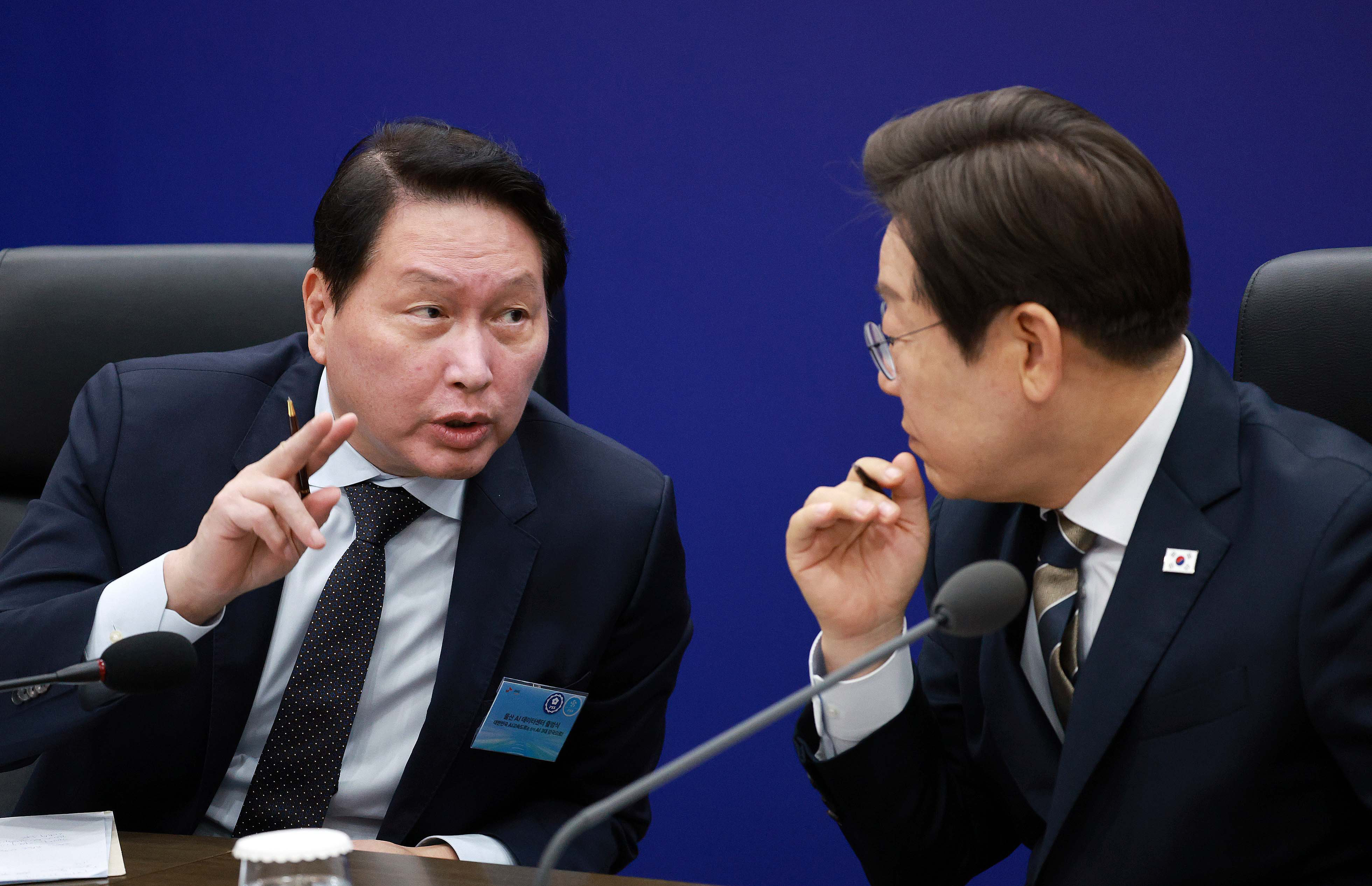
President Lee Jae-myung speaks with SK Group Chairman Chey Tae-won during the AI Global Cooperation Corporate Roundtable held at the Ulsan Exhibition and Convention Center on the 20th. 2025.06.20 Ulsan=Newsis
Samsung Electronics and SK hynix will establish a large-scale semiconductor cluster in Gwangju and Jeonnam. It will be the first time that an ultra-large semiconductor production complex encompassing both front-end fabs—the core of semiconductor manufacturing—and back-end processes will be built outside the Seoul metropolitan area. The investment amount is expected to reach several hundred trillion KRW.
According to political and business circles on the 23rd, SK Group Chairman Chey Tae-won is scheduled to visit Gwangju on the 30th and officially announce the “Gwangju-Jeonnam Semiconductor Cluster” initiative, centered on semiconductors and artificial intelligence (AI) data centers. In line with the launch of the integrated Jeonnam-Gwangju Metropolitan City on the 1st of next month, he plans to unveil a large-scale semiconductor investment. While investment had initially been expected to focus on back-end processes such as packaging, it is reported that the decision has been made to build a comprehensive semiconductor cluster in Gwangju and Jeonnam that includes front-end fabs, the core process that draws circuits on wafers. Chey is known to have presented this large-scale regional investment roadmap to President Lee Jae-myung in a meeting on the 19th. Samsung Electronics Chairman Lee Jae-yong is also expected to hold a closed-door meeting with the president on the 25th to finalize specific regional investment volumes, including in semiconductors.
The semiconductor industry estimates that more than KRW 100 trillion is required to build a single new front-end fab. As Samsung Electronics is also reviewing the construction of a fab in Gwangju, projections suggest that the combined investment of the two companies alone could exceed KRW 200 trillion.
Samsung–SK core semiconductor processes also in Gwangju–Jeonnam… Materials and equipment firms expected to follow
Semiconductor and other investments expected to spread beyond Seoul metro area
Key challenges: securing talent and component ecosystem
Lee Jae-yong likely to announce Chungnam investment on 2nd of next month
Chey Tae-won plans to unveil vision in Gwangju on 30th
Samsung Electronics headquarters in Seocho-gu, Seoul. Newsis
The move by Samsung Electronics and SK hynix to build a semiconductor cluster in Gwangju and Jeonnam is expected to mark a watershed in extending the advanced industrial landscape beyond the Seoul metropolitan area. If front-end semiconductor lines, which have so far been concentrated in metropolitan areas such as Yongin and Pyeongtaek in Gyeonggi Province, are established in Jeonnam and Gwangju, large numbers of materials, parts, and equipment (MPE) partners are also likely to relocate. This is expected to generate economic ripple effects, including job creation and higher tax revenues.
This investment is seen as the result of a combination of factors: surging demand for AI semiconductors, the physical limitations of infrastructure in the Seoul metropolitan area, and the push from political circles and local governments to avert the risk of regional decline. Existing semiconductor clusters in the metropolitan area, such as Yongin and Pyeongtaek, have been assessed as having reached physical limits in terms of power transmission and distribution networks and industrial water supply. On top of this, active lobbying by local governments that have staked their future on attracting advanced industries, together with the central government’s policy support, is seen as having contributed to the decision to invest in a Gwangju–Jeonnam semiconductor cluster. SK Group Chairman Chey Tae-won plans to announce the new semiconductor cluster project on the 30th alongside key government officials.
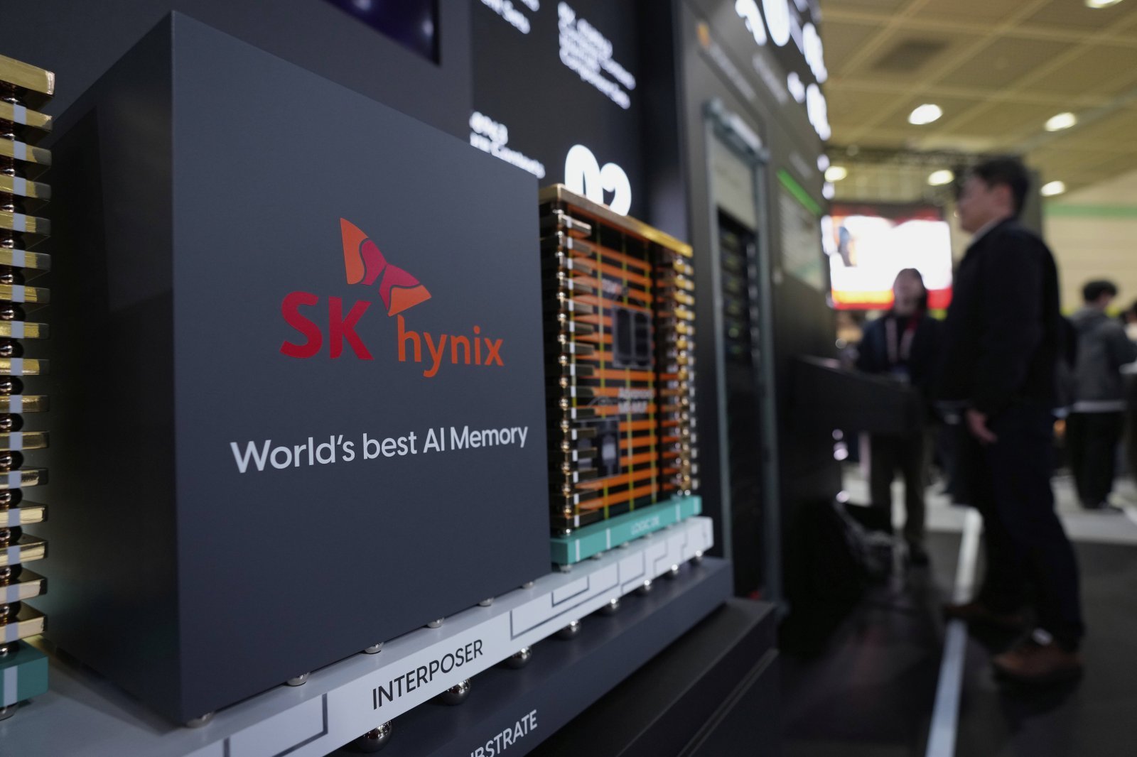
A model showing SK hynix’s high bandwidth memory (HBM) technology on display at the World IT Show held at COEX in Gangnam-gu, Seoul, on April 25, 2025. Seoul=AP Newsis
Particular attention is being paid to the fact that front-end fabs—the core of semiconductor manufacturing, which directly etch fine circuits on wafers—will be built, going beyond back-end processes. Front-end operations require the concurrent relocation of hundreds of MPE companies that supply chemicals and other inputs, as well as engineers capable of handling complex equipment. For this reason, semiconductor companies have adopted highly stringent criteria when selecting sites for new fabs. All conditions—power, parts, equipment, and talent—must be satisfied. Both Samsung Electronics and SK hynix operate memory fabs in China, but their advanced process facilities have been kept in the metropolitan area.
With the launch of the Jeonnam-Gwangju Metropolitan City and the establishment of a semiconductor cluster, the investment scale is expected to far exceed earlier projections. SK hynix is currently expected to invest around KRW 600 trillion to build four front-end fabs in the Yongin cluster. The semiconductor industry estimates that each front-end fab requires an investment of about KRW 100 trillion. In particular, because the Gwangju–Jeonnam region must build semiconductor infrastructure from scratch, it is projected that even a single fab would entail investment on the order of several hundred trillion KRW.
The large-scale regional investment starting in Gwangju and Jeonnam is expected to be followed from next month by announcements for other regions, including the Chungcheong and Gyeongsang areas. Large private-sector investments are taking shape around AI data centers in the Chungcheong region and around the space and aviation sector in the Gyeongsang region. Samsung Electronics Chairman Lee Jae-yong is widely expected to visit the company’s Cheonan campus in Chungnam on the 2nd of next month to personally announce regional investment plans, including the construction of an AI data center in the Chungcheong area. This is expected to be followed in early July by plans to build a space and aviation industry ecosystem in the Gyeongsang region.
However, in the case of the Gwangju semiconductor cluster, attracting talent and securing a robust components ecosystem are cited as major challenges. Concerns are also being raised that it may take five to ten years to optimize yields. Lee Jun-seok, leader of the Reform New Party, claimed on his social networking service (SNS) account on this day that “the Lee Jae-myung administration is twisting the arms of Samsung and SK hynix to send them to Honam,” adding that “political risk, which global investors dislike most, is at the core of the Korea discount.”
Meanwhile, on the 29th, the presidential office will host a working-level roundtable on regional investment with the participation of senior executives from major conglomerates. Attendees will include Jeon Young-hyun, head (vice chairman) of Samsung Electronics’ Device Solutions (DS) division. Participants are expected to brief the government on on-the-ground issues such as expanding power and water infrastructure to support large-scale regional investment, tax incentives, and measures to secure local talent.
ⓒ dongA.com. All rights reserved. Reproduction, redistribution, or use for AI training prohibited.
Popular News