Semiconductor / Samsung
Samsung to Mass-Produce First HBM4 After Lunar New Year
Dong-A Ilbo |
Updated 2026.02.08


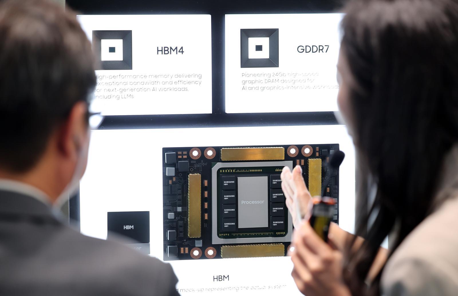
At the Samsung Electronics booth of the “K-Tech Showcase,” a side event of the APEC CEO Summit held at the Air Dome in Gyeongju Expo Park, North Gyeongsang Province, on the 28th, an attendee looks at HBM4. 2025.10.28. News1
Samsung Electronics is moving to secure its leadership in sixth-generation high-bandwidth memory (HBM), known as HBM4, as it receives strong interest from big tech companies. The company plans to begin mass production and shipment of products as early as the end of February, earlier than any other player in the industry, and to invest aggressively in HBM4 production facilities.According to the semiconductor industry on the 8th, Samsung Electronics is reportedly set to begin mass production and shipment of HBM4 for US-based NVIDIA from the fourth week of February, after the Lunar New Year holidays. If the schedule proceeds as planned, the company will become the first in the world to supply the latest HBM ahead of its competitors. Samsung Electronics stated during its earnings conference call for the fourth quarter of last year (October–December), held on the 29th of last month, that “at the request of major customers, HBM4 shipments are scheduled for February.” HBM4 will be mounted on NVIDIA’s next-generation AI chip “Vera Rubin.”
After having struggled in the HBM segment, Samsung Electronics has succeeded in winning recognition from big tech customers with HBM4, reshaping the market landscape. Up to the fifth generation (HBM3E), Samsung was the last among the three major DRAM makers—following SK hynix and US-based Micron—to pass quality testing. However, for HBM4, the company took a decisive step by adopting a process one node ahead of its rivals, and is now being assessed as having achieved the best performance in the industry.
While competitors developed HBM4 using 10nm-class (nanometer; 1nm is one-billionth of a meter) foundry (contract manufacturing) processes combined with fifth-generation (1b, 12nm-class) DRAM, Samsung differentiated its HBM4 by combining a 4nm foundry process with sixth-generation (1c, 11nm-class) DRAM. By using a more advanced process, the company improved product performance and power efficiency. This approach entailed a higher risk of development failure, but Samsung succeeded in passing validation by big tech firms such as NVIDIA. Samsung’s HBM4 delivers a data processing speed of 11.7Gb (gigabits) per second, far exceeding the standards of the JEDEC Solid State Technology Association and representing the highest level in the industry.
Samsung Electronics is also actively stepping up capital expenditure on facilities in line with strong HBM demand. According to industry sources, the company plans to build new DRAM production facilities at its latest fab, Pyeongtaek Line 4 (P4) in Gyeonggi Province, with a monthly capacity of 100,000–120,000 wafers. Samsung’s current DRAM production capacity is 660,000 wafers per month, and the addition of the new P4 facilities would increase this by about 20%. The company is expected to equip most of the expanded lines with 1c DRAM facilities dedicated to producing HBM4.
Samsung Electronics is openly expressing strong expectations for its HBM performance this year. In a recent conference call, the company stated, “This year’s HBM sales will improve significantly, tripling year-on-year,” adding, “Major customers hope to finalize supply agreements for subsequent volumes at an early stage, and we are actively making parallel investments to secure 1c production capacity.” As a result, forecasts are emerging that Samsung’s market share in the global HBM market will increase. KB Securities projected, “Samsung Electronics’ HBM market share is expected to double from 16% last year to 35% this year.”
Park Hyeon-ik; Lee Dong-hoon
AI-translated with ChatGPT. Provided as is; original Korean text prevails.
ⓒ dongA.com. All rights reserved. Reproduction, redistribution, or use for AI training prohibited.
Popular News