Samsung
Samsung Bets on HBM4 Mass Production Next Month
Dong-A Ilbo |
Updated 2026.01.26


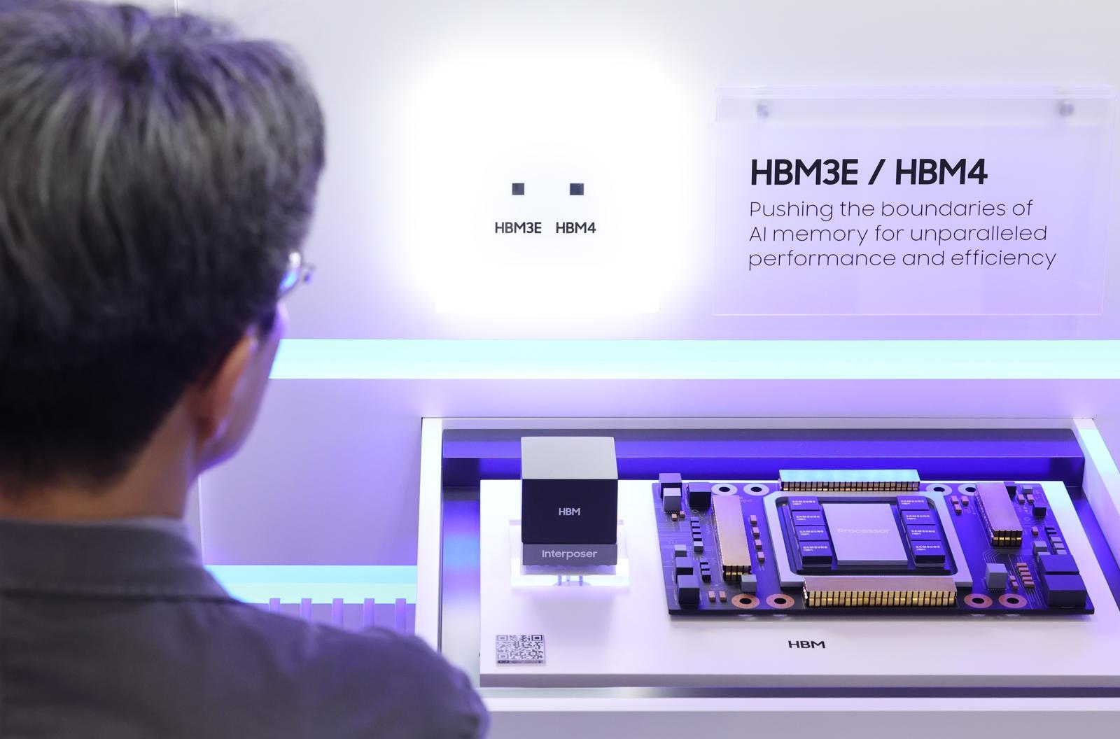
A visitor to the 27th Semiconductor Exhibition held at COEX in Gangnam-gu, Seoul, on 22 October last year looks at Samsung Electronics’ HBM4. 2025.10.22 Seoul=Newsis
Samsung Electronics will begin mass production next month of its sixth-generation high bandwidth memory (HBM), HBM4, which will be mounted on artificial intelligence (AI) semiconductors. After struggling in the HBM3 and HBM3E generations amid strong competition, the company is now assessed to be attempting to overturn the market in the sixth generation by playing a “super-gap” game changer.According to the semiconductor industry on the 26th, Samsung Electronics is expected to start mass production of HBM4 next month for supply to big tech customers such as Nvidia. HBM4 is a next-generation HBM that will be installed in the latest AI semiconductors, including Nvidia’s “Rubin” and AMD’s “MI450,” scheduled for release within the year.
Samsung Electronics’ HBM4 is said to show the highest performance level in the industry. Its data transfer speed reaches 11.7 Gb (gigabits) per second, far exceeding the 10 Gb per second demanded by the industry. The top speed of the previous-generation HBM3E was 9.6 Gb per second.
The high performance of Samsung Electronics’ HBM4 is seen as the result of implementing each semiconductor component of the product at the highest level. The logic die, which is located at the bottom of the HBM, connects DRAM and the graphics processing unit (GPU) and serves as the “brain” of the HBM, is designed using a 4-nanometer (nm; 1 nm is one-billionth of a meter) process, while the core component DRAM adopts the latest sixth-generation (1c, 11-nanometer-class) technology. SK hynix’s HBM4 consists of a 12-nanometer logic die and fifth-generation (1b, 12-nanometer-class) DRAM. As semiconductor process nodes become finer, integration density increases, which accelerates data processing speed and improves power efficiency.
Initially, the industry had evaluated that Samsung Electronics was taking on an excessive challenge. Having fallen behind competitors in the fourth- and fifth-generation HBM, namely HBM3 and HBM3E, there were widespread projections that it would be difficult for the company to stably realize performance by adopting technology that was considered too far ahead. Concerns were particularly strong regarding the logic die, where foundry (contract manufacturing) technology is key. Unlike SK hynix, which partnered with TSMC, Samsung Electronics opted to handle it with its own process, amplifying the worries. This is because TSMC is currently viewed as having an advantage over Samsung Electronics in foundry.
Samsung Electronics has dispelled these concerns, succeeding in bringing the performance and yield (ratio of non-defective products) of HBM4 onto a normal trajectory and gaining recognition from customers. Kim Dong-won, head of research at KB Securities, said, “Samsung Electronics’ HBM4 is expected to deliver industry-best performance.” Securities firms forecast that Samsung Electronics’ HBM market share this year will jump to the 30% range, about double its previous level.
The rise of competitors such as Google, Broadcom and AMD in the AI semiconductor market, which Nvidia has dominated, is another reason Samsung’s HBM4 is drawing attention. An industry official said, “Each company is trying to differentiate its products by using HBM with even slightly higher performance.” Samsung’s HBM4 is also expected to be mounted on Google’s next-generation AI chip, the Tensor Processing Unit (TPU).
Specific plans and schedules related to HBM4 are expected to become clearer during the earnings announcement on the 29th. On that day, Samsung Electronics and SK hynix will announce their results for the fourth quarter (October–December) of last year.
Park Hyeon-ik
AI-translated with ChatGPT. Provided as is; original Korean text prevails.
ⓒ dongA.com. All rights reserved. Reproduction, redistribution, or use for AI training prohibited.
Popular News