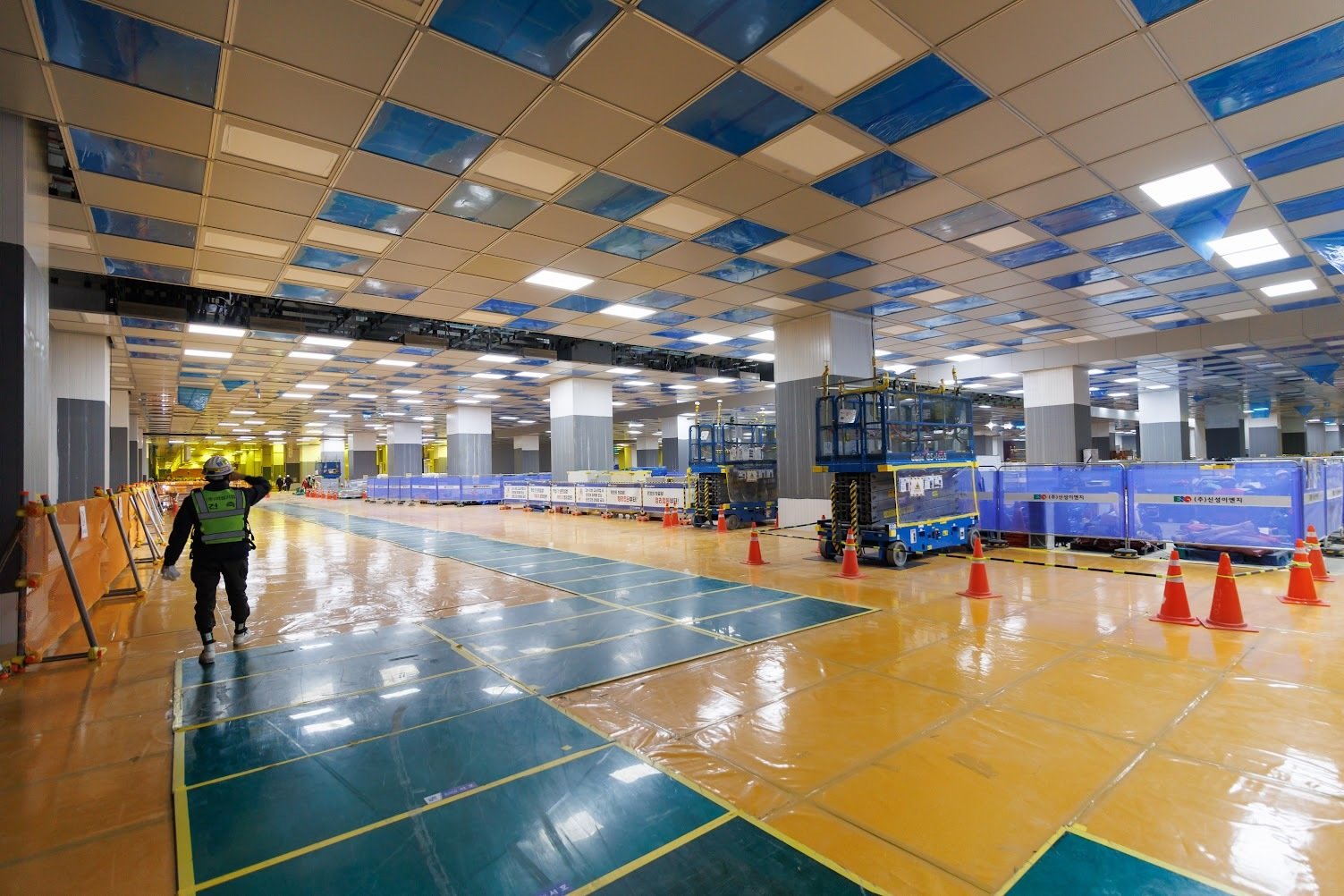
View of the SK hynix semiconductor fab under construction in Wonsam-myeon, Cheoin-gu, Yongin-si, Gyeonggi-do, on 11 August. 2026.8.11 News1
On the 10th, at the construction site of SK hynix’s Yongin Semiconductor Cluster, a next-generation memory production base located in Wonsan-myeon, Cheoin-gu, Yongin-si, Gyeonggi-do, work was in full swing attaching exterior materials to Yongin Cluster’s first fab (Y1) amid sand-blowing conditions. The construction progress rate is currently about 89%, with the first cleanroom scheduled to open in February next year and full-scale wafer mass production to begin in the fourth quarter (October–December).
After taking a construction lift installed inside the massive Y1 fab and getting off on the third floor, a space roughly half the size of a football field—about 1,000 pyeong (approximately 3,300㎡)—with exposed columns and ceiling pipes came into view.
This space is scheduled to be used as the “Trinity Fab,” which will be operational in the fourth quarter (October–December) of next year. It is a dedicated area inside the Y1 fab, which produces advanced memory, for verifying technologies developed by domestic materials, parts, and equipment (MPE) companies. As the AI semiconductor market expands beyond simple competition among individual companies into a broader “ecosystem” battle encompassing supply chains, a “mutual growth fab” is being opened to strengthen the competitiveness of domestic MPE firms.
● Targeting a 30% reduction in MPE products’ commercialization period The Trinity Fab is a performance verification facility established to shorten the commercialization period for domestic MPE companies, with a total investment of KRW 874.6 billion from the government, local governments, and SK hynix. Domestic MPE companies can conduct technology verification for new products by paying only minimal operating costs.
Until now, it has been practically difficult for MPE companies with limited financial resources to independently establish semiconductor verification facilities. Lee Jae-ho, vice chairman of TES, a front-end semiconductor equipment manufacturer, said, “A single measuring instrument costs around KRW 1 billion to KRW 5 billion, which is a significant burden for small and medium-sized equipment firms.”
Even when attempting to use production lines at semiconductor plants such as SK hynix or Samsung Electronics, product manufacturing necessarily takes priority, so on-site verification of MPE products has invariably been pushed to the back burner. Differences between the environment at verification facilities and that of mass production have also been a major challenge. Yoo Won-yang, CEO of TEMC, a producer of special gases for semiconductor processes, said, “There are cases where products pass verification at other institutions but fail to meet the actual mass production conditions of semiconductor manufacturers.”
Lee Ki-jeong, head of the Trinity Fab Foundation, said, “Because data obtained at the Trinity Fab is highly likely to be reproduced as is on actual mass production lines, it can ease the burden on companies,” adding, “The goal is to reduce by more than 30% the commercialization period—normally three to four years—for MPE companies’ products.”
● “New MPE technologies ultimately drive K-semiconductor competitiveness”
Interior view of the Trinity Fab. Provided by SK hynix
Inside the roughly 1,000-pyeong Trinity Fab, in addition to the central space that MPE companies use for mass production verification, 15 “mini cleanrooms” of about 13.6 pyeong each are arranged along the walls. These spaces can be used by MPE companies to test their own equipment or for research and development (R&D).
SK hynix has also introduced an “R&D Challenge Reward Program” for its partners. The initiative is based on the view that new MPE technologies ultimately translate into competitiveness for SK hynix. For MPE companies with strong technology ideas but insufficient initial funding, SK hynix will pay up to 50% of the upfront development costs in advance. Even if development fails or does not lead to procurement, compensation will be provided based on technological contribution and achievements.
Lee Hyun-cheol, vice president in charge of purchasing strategy at SK hynix, said, “We introduced this program to encourage our partners to take on future technology development more boldly,” adding, “We expect that our partners’ technology development will benefit SK hynix and, further, lead to stronger competitiveness across the entire semiconductor ecosystem.”
ⓒ dongA.com. All rights reserved. Reproduction, redistribution, or use for AI training prohibited.
Popular News