Chairman Lee Jae-yong visits the Yokohama “APL,” which opened in September, to review cutting-edge process research on-site
KRW 40 billion to be invested over five years
Aiming for technological synergies with Japan’s top-tier materials, components, and equipment ecosystem
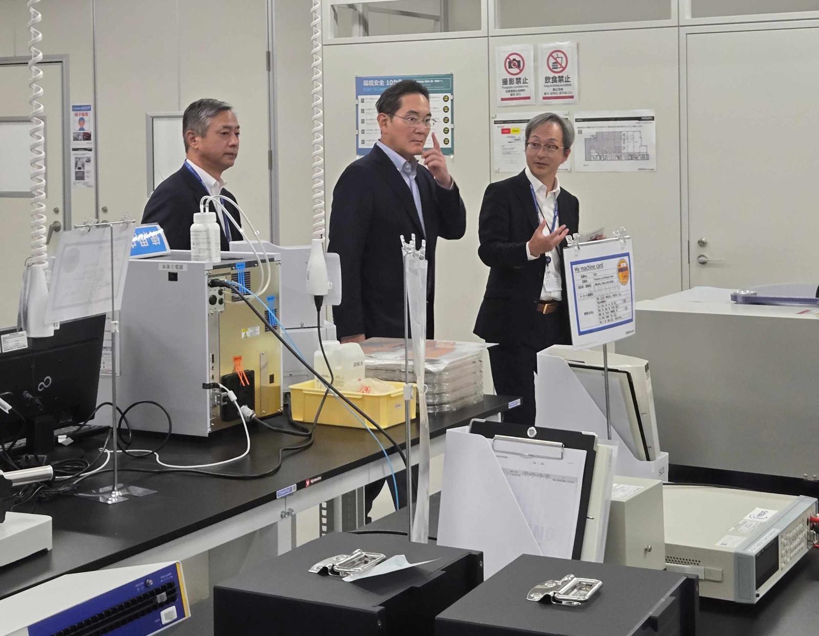
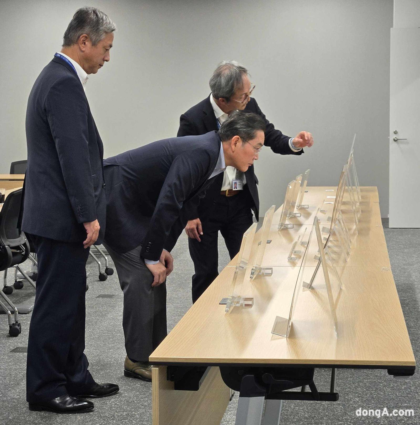
On November 1, Samsung Electronics Chairman Lee Jae-yong inspects the status of packaging technologies at Samsung Electronics’ advanced semiconductor packaging research hub, the Advanced Package Lab (APL), in Yokohama, Japan, together with Hiroichi Kawahira, Head of Samsung Electronics DS Research Japan Lab (Executive Vice President, to the left of Chairman Lee), Takashi Kariya, Head of APL Lab (Senior Vice President), and others. Provided by Samsung Electronics
On November 1, Samsung Electronics Chairman Lee Jae-yong visited the Advanced Package Lab (APL), an advanced semiconductor packaging research facility located in Yokohama, Japan, to directly review the progress of technology development. The on-site visit took place about two months after the lab officially went into operation in September.
During a meeting with local researchers, Chairman Lee checked the progress of next-generation package materials and process element technologies and discussed ways to expand points of contact with Japanese materials, parts, and equipment (MPE) companies. He reaffirmed the urgency of securing packaging technology capabilities, which determine semiconductor performance in the era of artificial intelligence (AI).
A hub linking semiconductor capabilities with Japan’s MPE ecosystemAPL is Samsung Electronics’ dedicated advanced packaging research hub established in Japan. Following the establishment plan in 2023, the company is investing a total of JPY 40 billion (KRW 350 billion) over five years from 2024 to build research infrastructure.
The lab is responsible for developing and validating basic materials and processes required for advanced packaging. It serves as a central axis that closely combines Samsung Electronics’ semiconductor design and manufacturing capabilities with Japan’s highly sophisticated MPE technology ecosystem.
APL plans to expand its research scope from wafer bonding technologies to future-oriented processes and materials such as glass substrates. It is also expected to lead the realization of next-generation packaging architectures for mass production of low-power, high-performance semiconductors optimized for AI environments. The lab will divide research domains with the packaging organizations under domestic semiconductor research centers to maximize synergies.
On November 1, Samsung Electronics Chairman Lee Jae-yong inspects the status of packaging technologies at Samsung Electronics’ advanced semiconductor packaging research hub, the Advanced Package Lab (APL), in Yokohama, Japan, together with Hiroichi Kawahira, Head of Samsung Electronics DS Research Japan Lab (Executive Vice President, to the left of Chairman Lee), Takashi Kariya, Head of APL Lab (Senior Vice President), and others. Provided by Samsung Electronics
Building a cooperation framework leveraging industry-academia-research infrastructure
Samsung Electronics’ decision to select Yokohama as a research hub is based on the city’s strong industry-academia-research infrastructure. Japan hosts a concentration of companies with world-class capabilities in semiconductor materials and equipment, and the government is actively pursuing support measures for the AI and semiconductor industries, providing an optimal environment for research and development.
Yokohama, with excellent access to Tokyo, is home to major universities and research institutes, offering advantages in securing specialized talent. It also hosts a cluster of MPE companies related to advanced packaging, enabling swift technological collaboration. Leveraging Yokohama’s talent pool and infrastructure, Samsung Electronics plans to steadily increase research staff and develop APL into a global core R&D hub for next-generation packaging.
Advanced packaging technology determines success in AI semiconductorsAdvanced packaging is regarded as a key technology that will shape the competitive landscape of the AI semiconductor market. This is because technologies that integrate multiple semiconductors—such as graphics processing units (GPUs), high bandwidth memory (HBM), and AI accelerators—into a single package determine overall system bandwidth, power efficiency, and heat dissipation performance.
In addition to its existing technological assets in memory and logic semiconductors, Samsung Electronics intends to strengthen the fundamental technologies for materials and equipment that are essential to implementing advanced packaging, thereby enhancing the competitiveness of its next-generation products.
ⓒ dongA.com. All rights reserved. Reproduction, redistribution, or use for AI training prohibited.
Popular News