[AI Robots Transforming K-Manufacturing] SK founded AI firm Gauss Labs six years ago Developed AI wafer virtual metrology solution… from sample checks to effectively 100% inspection CEO Kim Young-han: “Solving tough on-site challenges with AI”
“Semiconductors are the pinnacle of precision manufacturing. It was clear that if this challenge could be solved, it would set a benchmark for industrial artificial intelligence (AI).”
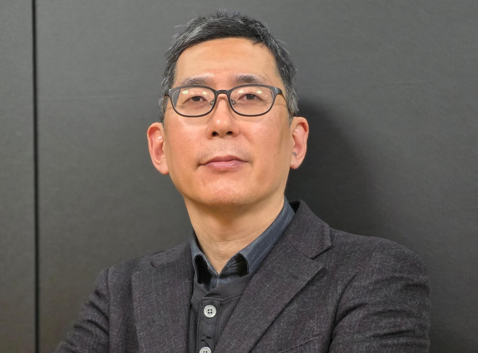
Gauss Labs CEO Kim Young-Han (photo) cited “semiconductor manufacturing” as the first domain that industrial AI should tackle. Gauss Labs was established and funded by SK in 2020 to foster AI technologies specialized for manufacturing and industrial sites.
Before founding Gauss Labs, Kim received his PhD from Stanford University in the United States and served as a professor in the Department of Electrical and Computer Engineering at the University of California, San Diego (UC San Diego). He was also a Fellow of the Institute of Electrical and Electronics Engineers (IEEE). What changed the course of his career was a sabbatical year spent at SK hynix in 2019. “There were many problems that could be solved when semiconductor data from the field was combined with AI,” Kim said.
With Kim’s participation, the SK Group began full-scale investment in industrial AI. Gauss Labs was launched with its headquarters in Silicon Valley, and SK hynix invested the entire initial capital of USD 55 million (about KRW 80.6 billion). The goal was to develop AI that could be used directly on semiconductor manufacturing lines.
The AI virtual metrology solution developed by Gauss Labs is called “Panoptes VM.” The name is derived from the giant with one hundred eyes in Greek mythology. It signifies constant monitoring and real-time analysis of every process in manufacturing. Development of the solution began in August 2020, and version 1.0 was released at the end of 2022. It has now been implemented on SK hynix mass production lines, where it virtually measures more than one wafer per second.
Semiconductor manufacturing consists of hundreds of processes, and each step requires a measurement process to verify the results. However, each piece of metrology equipment costs tens of billions of KRW, and processing times are long, so in reality only 1–5% of all wafers are inspected as samples. “The problem is that 95–99% of the wafers move on to the next process without anyone knowing whether they are defective,” Kim explained.
Panoptes VM analyzes data such as temperature, pressure, and gas flow collected from equipment sensors using AI to predict process outcomes without actual physical measurements. It generates virtual metrology values in real time immediately after a process is completed, achieving an effect close to 100% inspection. In the thin film deposition (“film”) and etching processes, where circuits are built up and etched on wafers, it has demonstrated about a 15% improvement in process variation. Variation refers to differences in individual process values that inevitably arise during semiconductor manufacturing; reducing this means higher uniformity in product quality.
Gauss Labs aims to expand its industrial AI innovation experience, accumulated in semiconductor fabs, into other industries. “Semiconductors are one of the most difficult industries in which to improve problems because the processes are complex and extremely fine, but success has an equally large ripple effect,” Kim said. “Solving this challenge and proving how industrial AI should operate in actual manufacturing environments is the direction Gauss Labs is pursuing.”
Lee Min-a
AI-translated with ChatGPT. Provided as is; original Korean text prevails.
ⓒ dongA.com. All rights reserved. Reproduction, redistribution, or use for AI training prohibited.