Highsemico Co., Ltd.
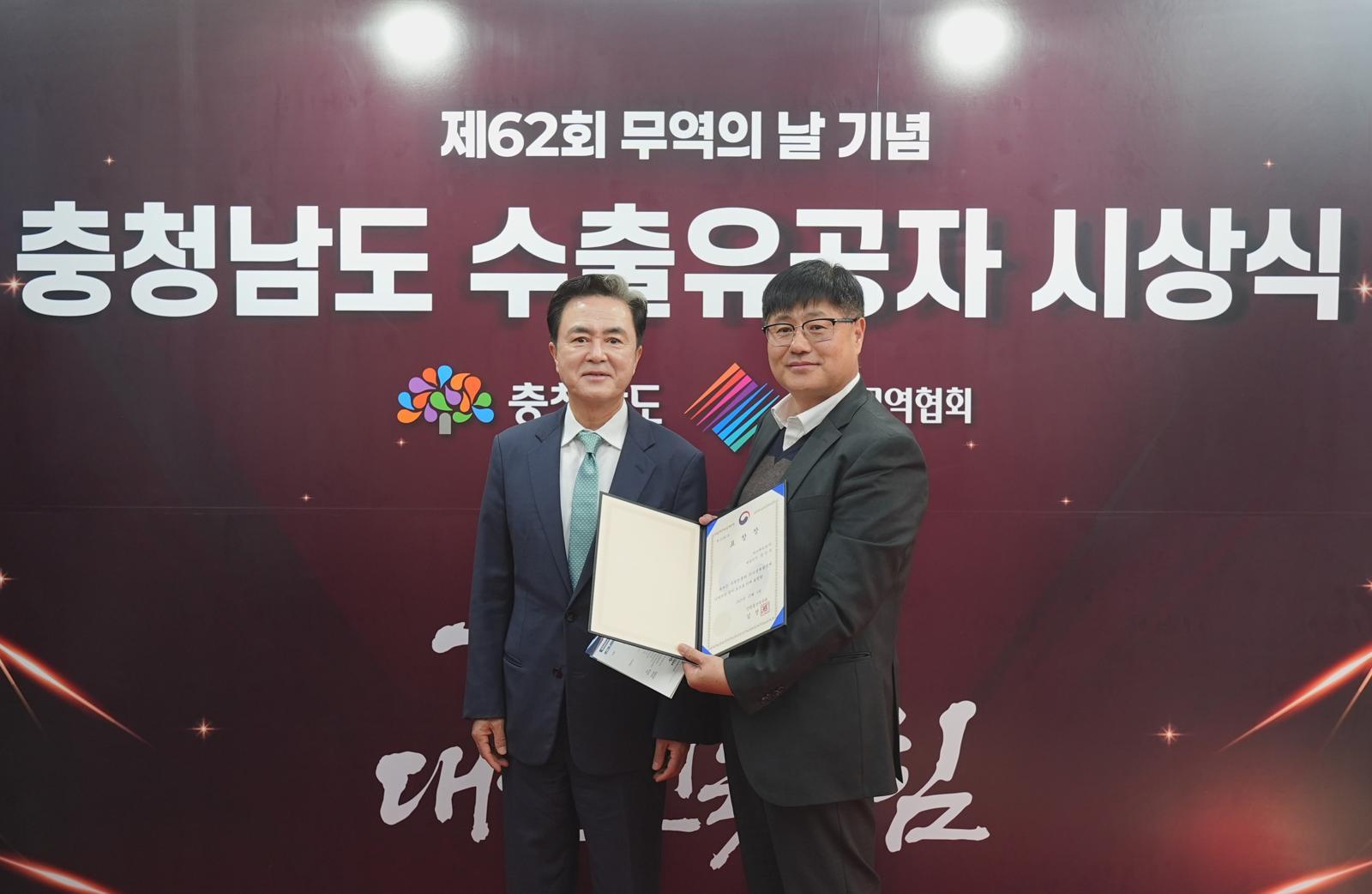
HISEMICO received the Minister of Trade, Industry and Energy Commendation on the occasion of the 62nd Trade Day. Kim Tae-heum, Governor of Chungcheongnam-do (left), and Han Min-seok, CEO of HISEMICO. Courtesy of HISEMICO
The glass core substrate market is rapidly emerging as a core technology for next-generation semiconductors, driving a surge in demand for related equipment. In particular, TGV (Through Glass Via) technology is regarded as an essential process for manufacturing advanced semiconductors such as AI semiconductors and HBM (High Bandwidth Memory), drawing attention in the global market. A domestic small and medium-sized enterprise has secured proprietary technological capabilities in this field and is moving to penetrate overseas markets, attracting significant interest.
HISEMICO Co., Ltd., a specialist in semiconductor and PCB surface-treatment equipment, is standing out in the industry based on its TGV technology. Founded in 2020, the company has, in just five years, engaged in technological cooperation with major domestic and global corporations and established itself as a leading player in the next-generation semiconductor equipment market.
In April this year, the company exported three pilot units incorporating TGV technology to a major Chinese corporation, gaining recognition for its technological capability. The TGV process is a core technology for mass production of glass core substrates, which are next-generation semiconductor substrates, and HISEMICO is the first company in Korea to commercialize it. The company is expanding its market by developing equipment applicable to the display market through a conformal method and to the semiconductor market for HBM through a full via method.
CEO Han Min-seok explained, “By building a one-stop solution that supports the entire metallization process in the TGV field—from laser hole processing to plating, etching, and CMP—through partner companies, we are dramatically shortening customers’ development periods.”
HISEMICO is also accelerating its efforts to enter global markets. In April last year, it opened a research laboratory in Suzhou, China, equipped with China’s first full-size 515×510 mm TGV metal plating test process for PKG. The company is currently conducting equipment and product evaluations with more than 50 major Chinese corporations, including Xiaomi, BOE, and Huawei, and some companies have progressed to the equipment quotation stage. In addition, as a bridgehead to target the Taiwanese TGV market, it has signed a business agreement with a large trading company and is working to secure local customers, using its participation in the 2025 TPCA Show in Taiwan as a starting point. Evaluations are already underway with some prospective customers.
In Korea, the company has established a TGV-dedicated research line at a major corporate research center and is producing metallization for various products based on key suppliers in the TGV supply chain, with evaluations underway for client companies.
The company’s growth based on technological strength has led to large-scale investment attraction. This year, it secured a growth momentum by passing the government’s DCP (Deep Tech Challenge Project) initiative. After conducting IR with 12 institutions over six months, it raised a first-round investment of KRW 3 billion on November 30 and received commitments for an additional KRW 12 billion in investment from four institutions, with final funding scheduled for January next year.
An investment industry source stated, “It is highly unusual for a small or medium-sized company, rather than a large or listed company, to attract investment of this scale,” adding, “This appears to reflect a strong assessment of the growth potential of the TGV market.”
The investment funds will be used for the construction of a new plant and the establishment of a post-plating inspection process. The company has completed the purchase of a 1,900 m² site in an industrial complex located five minutes from the North Cheonan interchange. It plans to build a manufacturing plant with cleanroom facilities and office space, with construction scheduled to begin in March next year and move-in targeted for October.
The company also plans to continue technology development. HISEMICO will promote a joint project with Seoul National University of Science and Technology and the Korea Electronics Technology Institute to develop automation for semiconductor plating equipment, supported by KRW 3.6 billion in government funding over three years. Through this, the company aims to launch stable mass-production equipment for 8-inch and 12-inch wafers and enhance the price and delivery competitiveness of domestic small and medium-sized OSAT (Outsourced Semiconductor Assembly and Test) companies.
The company is also actively contributing to the revitalization of the display and semiconductor ecosystem in the Chungnam region. It successfully held a TGV technology seminar in cooperation with Chungcheongnam-do, Hoseo University, and existing participating companies, and plans to create a new TGV market ecosystem in the region by holding regular quarterly forums starting next year.
CEO Han emphasized, “With the current semiconductor ecosystem concentrated in the Seoul metropolitan area, there are many TGV demand companies in Chungnam and Daejeon,” adding, “If project support for locally based companies is strengthened and the investment ecosystem is improved, this will lead to regional economic development.”
Recognizing its achievements to date, HISEMICO received the Governor of Chungcheongnam-do Commendation last year, as well as the Grand Prize in the Quality Innovation category at the Korea SME and Mid-sized Enterprise Awards and the Minister of Trade, Industry and Energy Commendation on Trade Day this year. CEO Han stated, “The company will continue to lead the global semiconductor surface-treatment equipment market with innovative technologies.”
ⓒ dongA.com. All rights reserved. Reproduction, redistribution, or use for AI training prohibited.
Popular News