[Seoul Startup Hub x ITDongA] Challenge K-Startup is the largest startup competition in Korea, jointly organized by 10 government ministries and agencies. Among them, the Seoul Center for Creative Economy & Innovation operates the General League of the Innovation Startup League. ITDongA looks into promising startups that have grown together with the Seoul Center for Creative Economy & Innovation.
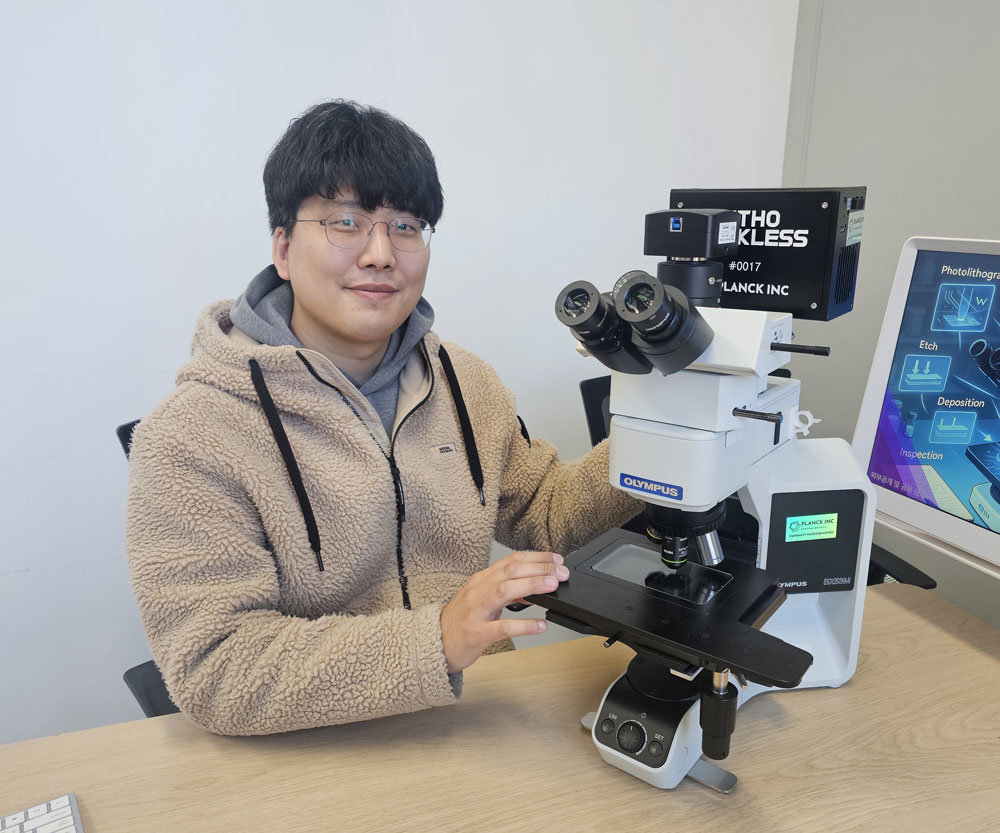
CEO Kim Seok-beom of Planck Lab / Source=ITDongA
In semiconductor development, the lithography process is extremely important. It is the step that forms the fine circuit patterns required for semiconductor chips on a substrate. However, conventional lithography processes were structured to rely on a consumable called a “photomask.” A photomask is a kind of template in which the pattern to be projected is embedded, and a new mask was required each time a test was conducted. The time and cost involved were substantial.
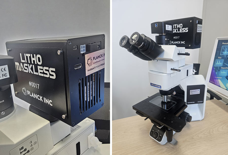
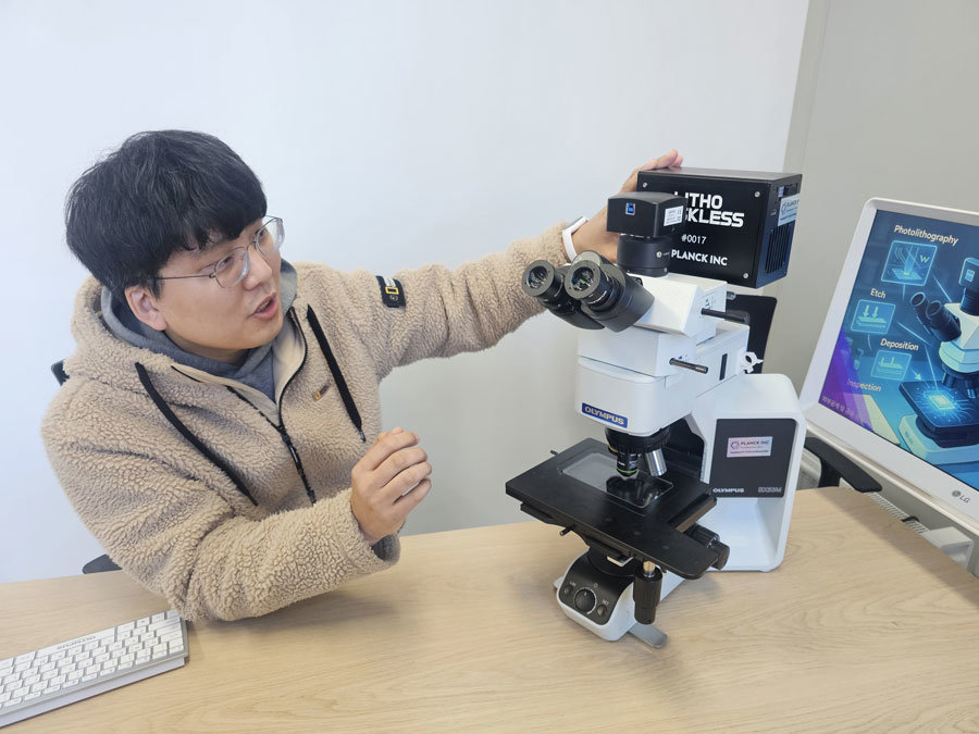
Planck Lab (CEO Kim Seok-beom) is addressing this problem. By introducing a digital lithography system, “MASKLESS LITHO,” which can expose semiconductor circuit patterns onto a substrate without a photomask, the company is driving the digital transformation of semiconductor development. Since its incorporation in July this year, it has supplied more than 50 units to four countries: the United States, Australia, Singapore, and Russia. ITDongA met with CEO Kim Seok-beom of Planck Lab, which is growing together with the Seoul Center for Creative Economy & Innovation, to hear about the company’s technology and business strategy.
- Starting a business in semiconductors is not something just anyone can do. What path led to launching this startup?: All of my bachelor’s, master’s, and Ph.D. degrees in mechanical engineering are from Sogang University. My research areas are MEMS (Micro-Electro-Mechanical Systems) and SLA-based photocurable 3D printing (stereolithography).
In fact, this is not my first startup. In 2014, during my master’s program, I co-founded a photocurable 3D printer company called “Illuminaid,” and we mass-produced one of Korea’s first DLP-based dental 3D printers and supplied them to major dental companies such as MegaGen. The company’s technological capabilities were recognized, and it was incorporated as a subsidiary of Daewoong Group, then later acquired by CGBio, through which I experienced my first exit (the founder sells their shares and leaves the company).
- If a startup went as far as an M&A, would that not be considered a successful case in its own right?: It could be seen that way, but to be honest, on a personal level I do not think it was a major success. At the time, I only understood “founding a company,” and I lacked a business mindset. I did not know how to raise investment, nor how to handle things like management control disputes. I knew the technology, but I was not familiar with marketing or management. I still regret not being able to pursue a bigger vision because of that.
Afterward, I began looking for a new path where I could break away from the rigidity of a large corporate system and freely pursue my ambitions. However, I was afraid to start a business again right away, so I worked for three years as a technical director at a startup, where I gained experience in software technology and accumulated know-how. Building on that experience up to this May, and on three foundations—the hardware and software data I had accumulated, and my major in semiconductors—I founded Planck Lab on July 1 this year.
- The company name Planck Lab is quite unique. What does it mean?: The name Planck Lab is derived from Max Planck (1858-1947), the founder of quantum mechanics. Just as Max Planck changed the paradigm of physics through quantum mechanics, Planck Lab aims to change the paradigm of semiconductor processes with digital maskless technology.
- What kind of company is Planck Lab, and what specific solutions does it offer?: Simply put, Planck Lab develops equipment that helps manufacture micro-sized patterns or objects. Among these, our current focus is on a system called “MASKLESS LITHO,” which applies maskless lithography technology. The advantage of this product is that it achieves low cost yet high performance by combining the correction and graphics technologies I experienced at a software company.
Maskless lithography is literally the same technology used in movie theater projectors. If a cinema projector is a technology that displays RGB colors, we use the same principle but work with UV (ultraviolet). We project ultraviolet light as images in the desired shapes. While movie theaters use the technology to greatly enlarge the image, we have the technology to reduce it to a small scale.
- It is said to be based on DLP technology. Is this not the technology mainly used in projectors? Is it common for DLP technology to be used in fields other than entertainment?: That is correct. We are based on TI (Texas Instruments) DLP technology, which has been verified in the global projector market. We also use TI’s DMD (Digital Micromirror Device) chips.
In fact, there are teams overseas that apply this technology in the semiconductor sector as well. It can be called a recent trend. However, while DLP technology has been used in existing research-purpose solutions, they were mostly excessively expensive imported systems, which posed limitations.
- Why is such precise projection technology needed in the semiconductor industry? And what differentiates your product from existing ones?: Conventional lithography equipment has been used to form the precise circuit patterns required for semiconductor design and production. However, it has been very expensive and inefficient. It could only expose fixed patterns, and a consumable called a mask was always required.
A mask is like a template in which the pattern to be projected is embedded. The shape of the pattern we want to create is formed on a glass substrate; when light is shone through it, the areas with patterns block the light, and the areas without patterns allow it to pass. Every time the mask is changed, it costs money. Since a new mask must be made whenever the experimental pattern changes, the time and cost required were substantial.
Our product, however, can perform exposure directly from the image itself. Because it can expose exactly in the shape of the image, it is easy to draw and immediately expose. Circuit patterns can be easily created and exposed onto a substrate using general-purpose software such as Microsoft Paint or PowerPoint.
- In a way, it sounds similar to the digital transformation of the film industry. Did cinemas not also need analog film in the past?: It is an accurate analogy. In the past, analog projectors in movie theaters required a massive amount of film to screen or produce a new movie. The film was difficult to transport, and everything—storage, management, and use—was inconvenient. It was also very costly.
Today, theaters use digital projectors. Because the system is based on digital data, it is efficient in every aspect, from content production and duplication to management and screening. Our MASKLESS LITHO offers similar advantages. Just as cinema screens underwent a digital transformation, the semiconductor industry can also achieve a complete digital transformation through this technology.
MASKLESS LITHO from Planck Lab integrated with an existing microscope / Source=ITDongA
- It is said that this technology can save a significant amount of cost. It is particularly noted that it can be combined with existing microscopes?: There are many microscopes in laboratories that, although installed, are not actually used. A major advantage of our product is that such equipment can be upcycled and reborn as higher value-added infrastructure.
In the conventional environment, semiconductor work required a facility called a clean room. Our product, by contrast, only requires a microscope, making it possible to fabricate and test semiconductors easily in a small space.
- Compared with existing environments, what is the scale of cost savings?: Compared with existing environments where a clean room was needed, the setup cost is roughly one-tenth. Clean rooms are very expensive to build, and cumbersome to maintain. Many laboratories and universities do not even have the physical space. Since our product is not intended for so-called cutting-edge semiconductor fabrication, such high-cost facilities are not necessary. A dust-free development environment can be set up with the addition of simple accessories.
- How does the precision compare with that of conventional lithography equipment?: There is an existing product called a mask aligner, and our system can achieve equivalent or even superior performance compared with that equipment. It supports patterns as fine as 600 nanometers at best, and it is very easy to develop patterns with an average feature size of 1 micrometer.
- In which fields is this product particularly useful? What is the current market response?: It is very useful for small and medium-sized enterprises (SMEs) and educational institutions. It is suitable for institutions such as universities or SMEs that, rather than mass-production, want to quickly create a variety of products, or that want to conduct hands-on training in semiconductor processes. In fact, the Korea Science Academy of KAIST is currently using our product for semiconductor education.
In the research-use market, it is receiving highly favorable reviews and is rapidly replacing existing products. We have sold more than 50 units to universities and research institutes in four countries around the world—the United States, Australia, Singapore, and Russia. Considering that we only established the corporation in July this year, this is quite a solid achievement.
In particular, the research team led by Toby Shannelly at UTS (University of Technology Sydney) in Australia highly evaluated our product, noting that it has exponentially increased their research speed and that its ease of use allows a wide range of users to adopt it readily. In addition, the research team of Professor Jung Moon-seok in the Department of Physics at Hanyang University in Korea praised it as an indispensable piece of equipment for semiconductor research using two-dimensional materials.
Furthermore, Dr. Yoon Yeo-won at USC (University of Southern California) in the United States also evaluated our product highly for its versatility, saying that it is suitable even for bio applications. Thus, we are receiving positive feedback both domestically and overseas.
- After achieving results in the research-use market, do you plan to expand into industrial applications?: Yes. Our current product is for research use, but after establishing a track record in the research market, we plan to expand into industrial applications. Industrial products can be applied across a wide range of fields. It can be extended to all industries requiring UV-based patterning processes, including bio, packaging, sensors, and microdisplays. We aim to unveil full-fledged industrial results in the second half of next year. Through this, we expect to attract attention in the semiconductor and display markets.
- Many startups struggle with practical issues such as personnel and costs, even if they possess strong technology. Planck Lab likely faces similar challenges. How have you addressed them?: First, there is the talent issue. Our product does not rely on just a single technology; it is based on converged and compound technologies. Therefore, recruiting experts in each of these areas is the most difficult. Also, while our ultimate target customers are large corporations such as Samsung and SK Hynix, in the current situation it is not easy to build the networks—namely, the sales channels—needed to sell to such conglomerates. For this reason, we are first focusing on the research market, while in parallel preparing full-scale industrial products. We hope that people who use our product at research institutes or educational institutions will have a favorable view of us later on when they join large companies.
- What are your impressions of the support programs from the Seoul Center for Creative Economy & Innovation?: With support from the Seoul Center for Creative Economy & Innovation, we were the only team from the Preliminary Startup League to advance to the Grand Finale of Challenge K-Startup. We also finished in 5th place and received the Minister of National Defense Award. Many of the companies in the preliminary startup category do not have a strong technological base, and we achieved an almost unparalleled result among them.
The Seoul Center for Creative Economy & Innovation provided extensive support for this, including IR consulting and various other advisory services. They also connected us with a range of investors through their networking efforts. In addition, they supported our PR and marketing, helping us to attract investment smoothly.
As mentioned earlier, many entrepreneur-engineers have strong technological capabilities but struggle because they are less familiar with marketing or management. The support programs of the Seoul Center for Creative Economy & Innovation appear to be of great help to such people.
CEO Kim Seok-beom of Planck Lab / Source=ITDongA
- Any future plans or additional messages you would like to share?: Planck Lab is currently carrying out various activities targeting several countries, including the United States and Vietnam, in preparation for global expansion next year. We have already signed a significant number of contracts, and expectations are rising. Riding this momentum, we are confident that the day will come when we are recognized as a solid export company.
We have already secured distributors in three countries and plan to attract partners in more countries to expand our global exports. We intend to successfully complete our ongoing seed investment round and accelerate our entry into the B2B market by strengthening our technical workforce, mass-production capabilities, and global sales network.
We are confident that we will rise to prominence not only in the research-use market but also in the full-fledged industrial market in the future. Beyond the research sector, we seek to apply digital maskless technology across diverse fields such as advanced semiconductor packaging, HDI PCBs, OLED, and sensors, thereby driving innovation throughout the semiconductor industry. We look forward to continued interest and support.
Reporter Kim Young-woo, ITDongA (pengo@itdonga.com)
ⓒ dongA.com. All rights reserved. Reproduction, redistribution, or use for AI training prohibited.
Popular News