Boston Dynamics humanoid robots “Pilot testing at a U.S. semiconductor plant next year” Additional deployment of ‘Spot’ quadruped robots
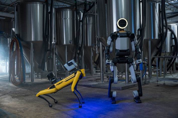
‘Atlas’ (right), a humanoid robot and ‘Spot’, a robotic dog, from Boston Dynamics that will be deployed early next year at the semiconductor production sites of GlobalFoundries. Courtesy of Hyundai Motor Group.
‘Atlas’, the humanoid robot developed by Boston Dynamics, the robotics affiliate of Hyundai Motor Group, is set to expand its scope of activity from finished vehicle manufacturing plants to semiconductor production lines.
Boston Dynamics announced on the 17th (local time) that it will promote a pilot test by deploying Atlas from early next year at the production sites of GlobalFoundries, a U.S. semiconductor foundry (contract manufacturing) company. The quadruped robotic dog ‘Spot’, which has already been in operation, will be deployed additionally.
With this, GlobalFoundries has become the first customer outside the finished vehicle industry to verify the performance of Atlas. Previously, Hyundai Motor Group stated that it would deploy Atlas at Hyundai Motor Group Metaplant America (HMGMA) in Georgia, U.S., in 2028.
Boston Dynamics will begin on-site testing of Atlas early next year at GlobalFoundries’ major facilities around the world. It will first identify workstations within semiconductor manufacturing environments where humanoid robots can be utilized. After pinpointing these specific work areas, the company plans to conduct initial testing and artificial intelligence (AI) training for Atlas to perform its missions.
Spot, which has already been deployed at GlobalFoundries’ Vermont plant in the United States, will see its application scope expanded. It will also be deployed at plants in New York, U.S., and Dresden, Germany. Having operated Spot at the Vermont plant for more than four years, the company recently introduced Spot to its Singapore facility as well. Since April this year, two Spot units deployed at the Singapore plant have traveled approximately 900 km within the “sub-fab” area beneath the cleanroom where semiconductor manufacturing processes are carried out, performing 99% of more than 90,000 equipment inspection tasks. The sub-fab is the space directly below the main cleanroom that supplies air and electricity so that the main cleanroom can carry out dust-free semiconductor etching operations.
Choi Won-young
AI-translated with ChatGPT. Provided as is; original Korean text prevails.
ⓒ dongA.com. All rights reserved. Reproduction, redistribution, or use for AI training prohibited.