3D-stacked HBM on AI accelerators shortens data travel distance to boost performance
Triple power efficiency, half the thermal resistance… debut of 8-layer V-NAND “zNAND-O”
“Korea will retain the memory crown through 2031… but cutting new product development cycles by 12 months is a burden”
As artificial intelligence (AI) evolves from simply answering questions to functioning as actual task-performing “agents,” the importance of memory semiconductors that enable contextual understanding and reasoning in conversations is growing. With competition intensifying for the high-value-added memory market, Samsung has unveiled a new type of memory that stacks high bandwidth memory (HBM) directly on top of an AI accelerator.
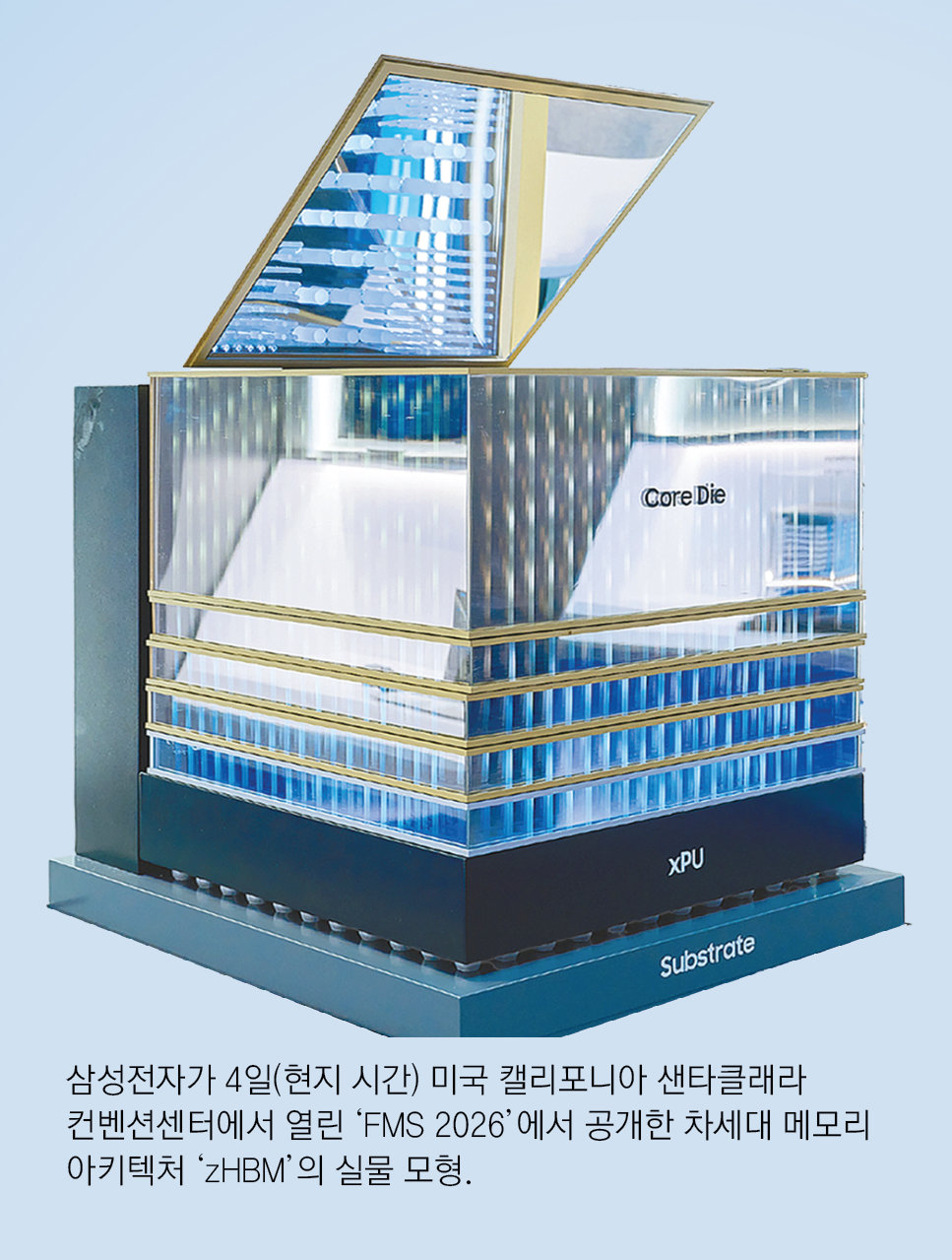
On the 4th (local time), Samsung Electronics presented a physical mock-up of “zHBM,” a next-generation three-dimensional (3D) memory architecture, at “FMS 2026,” held at the Santa Clara Convention Center in California, United States. FMS 2026 is the world’s largest memory-focused conference and a major event attended by all key memory semiconductor manufacturers.
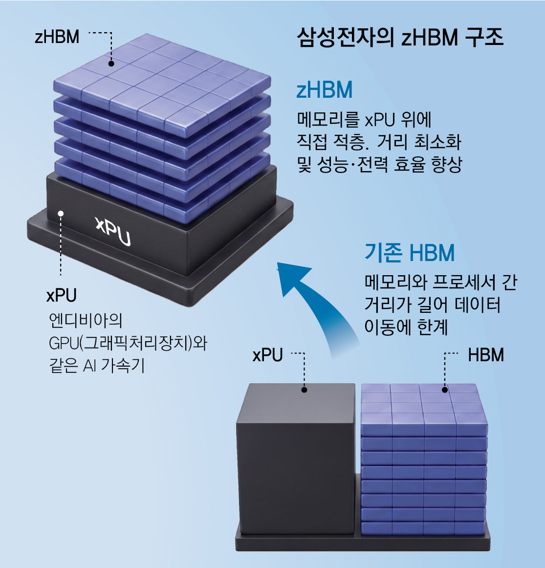
The zHBM unveiled by Samsung Electronics stacks HBM vertically on top of an AI accelerator (xPU). The prefix “z” was added to signify the use of height (Z-axis), rather than just the two-dimensional width and length (X·Y axes). Whereas HBM was previously stacked next to the xPU, it is now placed above it, reducing the physical distance between the xPU and the memory. In effect, the previous approach of connecting the memory and compute units with a “bridge” has been replaced by integrating them like upper and lower floors of the same building.
As the physical distance is reduced, data stored in memory can be transferred to the xPU much more quickly. Samsung Electronics stated that a next-generation system adopting zHBM achieves a data processing speed eight times higher than a system using HBM5. Performance per watt is improved threefold, while thermal resistance is reduced to less than half.
Samsung Electronics and SK hynix are also stepping up efforts on technologies using NAND flash. On the same day, Samsung Electronics additionally unveiled a physical mock-up of “zNAND-O (zNAND-O),” which stacks the latest V-NAND in eight tiers. Earlier, SK hynix and SanDisk announced the first standard for high bandwidth flash (HBF), a next-generation storage technology.
If HBM is a technology that vertically stacks DRAM, HBF maximizes performance by stacking NAND. NAND can store more data due to its structure and, as a non-volatile memory, does not require additional current to maintain data, enabling operation with lower power consumption.
Based on the two companies’ technology development, the industry expects that Korea will maintain its leadership in the memory semiconductor market at least through 2031. Josephine L’Ho, an analyst at French market research firm Yole Group, presented this outlook at FMS 2026, citing as grounds the Korean government’s plan to double wafer output within five years and the aggressive investments by Samsung Electronics and SK hynix.
However, she also pointed out that in the rapidly changing AI development environment, the shortening of new product development cycles for memory manufacturers from 18 months to 12 months could become a burden. As development speed is a key source of competitiveness, only companies that respond nimbly to market dynamics are likely to survive.
ⓒ dongA.com. All rights reserved. Reproduction, redistribution, or use for AI training prohibited.
Popular News









 About Dong-A Ilbo