The clear biggest beneficiary of the artificial intelligence (AI) boom shaking the world is “semiconductors.” Among them, high bandwidth memory (HBM), which has dramatically increased data processing speed, has become an indispensable component for advancing AI performance, sending manufacturers into an unprecedented boom. Global big tech companies are literally lining up with cash in hand to secure HBM supply.
However, semiconductor manufacturers are not the only ones smiling in the HBM boom era. Companies that produce the core equipment essential for semiconductor manufacturing are also enjoying a strong trickle-down effect. Competition to preempt the market is equally intense. Hanwha Group has now fully entered this fiercely contested equipment market.
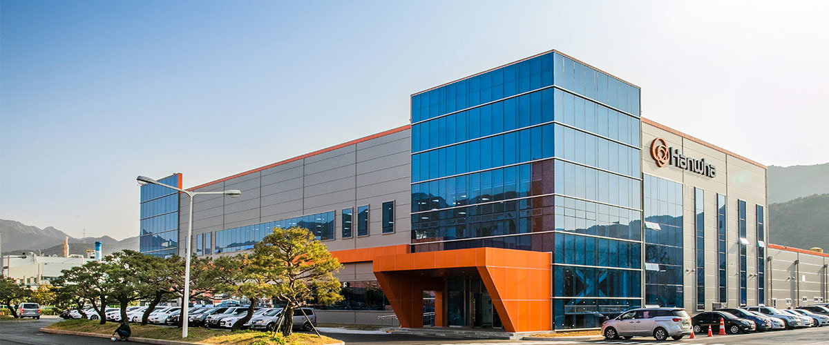
View of Hanwha Semitec.
At the forefront is Hanwha Vision. The company is accelerating its transition from a CCTV and video security-centered business to a semiconductor equipment enterprise. As a latecomer to the core HBM manufacturing equipment market, Hanwha Vision is drawing attention in the industry over whether it can leverage its technological capabilities to secure a firm position as a “player” in the semiconductor equipment sector.
From security firm to semiconductor equipment maker… evolution of 30 years of ultra-precision technology
Hanwha Vision is a global video security solutions company that has continued its video security business for more than 30 years since launching its first security camera in 1990. Last year it posted revenue of KRW 1,790.9 billion and operating profit of KRW 162.3 billion, and 88% of its security business sales were generated overseas, underscoring its solid foothold in the global market. Hanwha Vision is now seeking to shed its existing image as an optics and security company and transform itself into a semiconductor equipment enterprise.
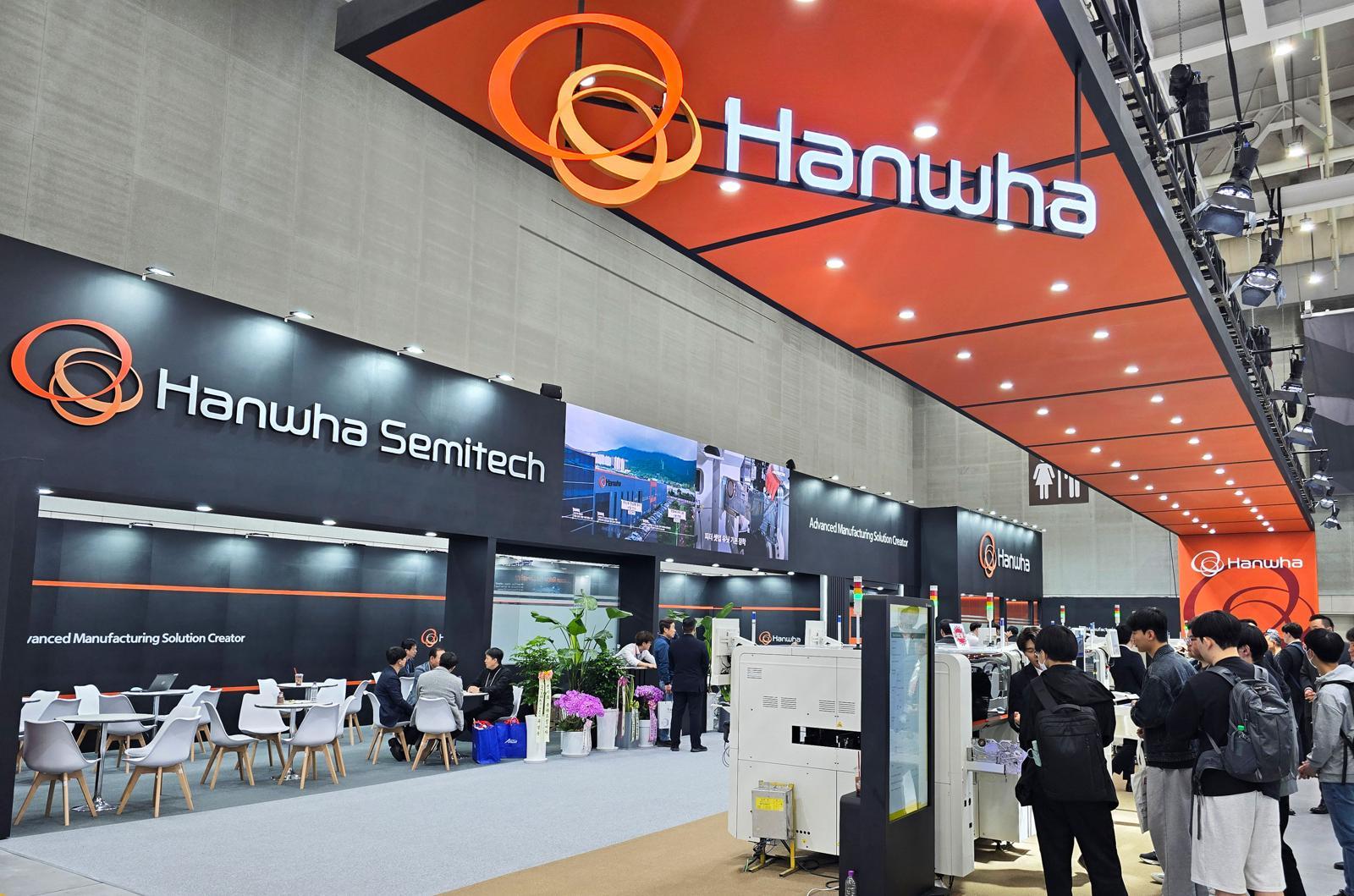
Hanwha Semitec participated in the country’s largest surface mount technology (SMT) exhibition, which opened at Suwon Convention Center in Gyeonggi-do. Provided by Hanwha Semitec.
At the core of this shift is “Hanwha Semitec.” Hanwha Semitec is a wholly owned subsidiary of Hanwha Vision. It did not belong to Hanwha Group from the outset. Its origins trace back to Samsung Precision Industries, founded in 1977, which later changed its name to Samsung Techwin and expanded into defense, aerospace, CCTV, optics and precision machinery. In 2014, however, Samsung Techwin was acquired by Hanwha Group and renamed Hanwha Techwin. Subsequently, the defense business was spun off to Hanwha Aerospace, CCTV and related businesses to Hanwha Vision, and precision machinery and related operations to Hanwha Precision Machinery.
Its ties with semiconductors go back further than many assume. In 1989, it launched Korea’s first surface mount technology (SMT) chip mounter business, and in 1993, it introduced its first semiconductor back-end process equipment, a wire bonder. In January 2024, it expanded its portfolio by acquiring front-end semiconductor business from Hanwha Momentum, and in February last year it changed its name from “Hanwha Precision Machinery” to “Hanwha Semitec,” signaling a new beginning as a specialist semiconductor equipment company.
Breaking through SK hynix’s qual test… “TC bonder” that secures HBM yield
The key driver of Hanwha Semitec’s current growth is its “TC bonder.” HBM is manufactured by vertically stacking multiple DRAM dies; even a minute misalignment of the chips can drastically reduce performance, making precision a direct source of competitiveness. The TC bonder is the equipment that inserts bumps (conductive protrusions) between chips and applies heat and pressure to bond them together. As HBM demand increases, the need for TC bonders grows in tandem.
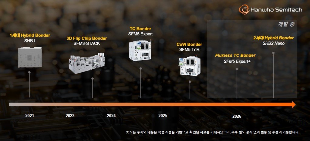
Hanwha Semitec’s advanced semiconductor packaging equipment development roadmap.
Despite entering the market as a latecomer, Hanwha Semitec has been rapidly raising its profile. It began full-scale development of TC bonders in 2020 and, four years later in 2024, developed the “SFM5 Expert.” In March 2025, it passed SK hynix’s quality verification (qual test), enabling mass production of the product. Last year, Hanwha Semitec secured a contract worth about KRW 80.5 billion to supply TC bonder equipment to SK hynix, emerging as a new supplier in a market that had effectively been a monopoly. Early this year the company reportedly signed an additional equipment supply contract worth around KRW 9.7 billion, and is now seen as introducing a meaningful crack in the previously rigid market structure.
Hanwha Semitec explains that the ultra-precision control technology it has accumulated over decades in its existing core SMT chip mounter business underpinned TC bonder development. A company representative said, “There are similarities between SMT and semiconductor back-end process equipment, which allows us to share R&D capabilities and has greatly helped diversify back-end semiconductor packaging methods.”
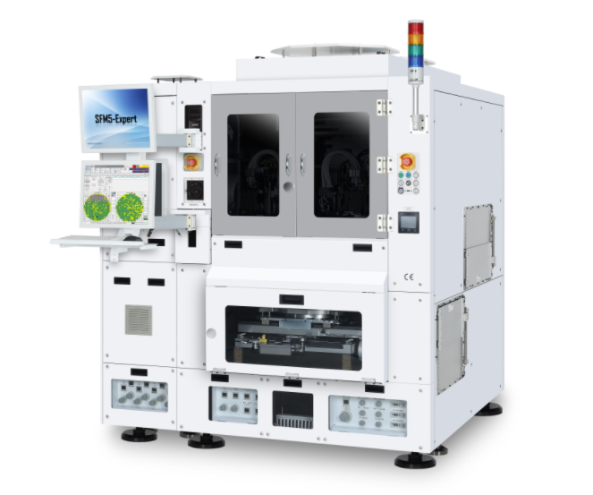
Hanwha Semitec TC bonder SFM5 Expert. Provided by Hanwha Semitec.
A Hanwha Semitec representative also appeared on a YouTube channel last year to directly explain the differentiating factors of its TC bonder. According to the company, it has applied high-end components to increase units per hour (UPH), introduced special composite materials for heat and vibration control, and developed proprietary control modules and algorithms instead of using commercial software to enhance compatibility between equipment and software.
Development is also in full swing on a second-generation TC bonder targeting the next-generation HBM equipment market. In particular, this year the company plans to introduce a TC bonder with an enlarged bonding head, as well as a fluxless TC bonder that reduces the gap between chips.
Next battleground: “hybrid bonder”… aiming for an ultra-gap with 0.1 μm precision
The area where Hanwha Semitec is currently focusing most heavily is “hybrid bonding,” regarded as a core technology for the next-generation semiconductor packaging market. The higher HBM stacks DRAM dies, the more data it can process. However, as the number of layers increases, process complexity also rises, demanding extremely precise bonding technology. While TC bonders have so far been established as the standard for HBM manufacturing, they are widely viewed as having limitations in producing highly stacked chips of more than 20 layers.
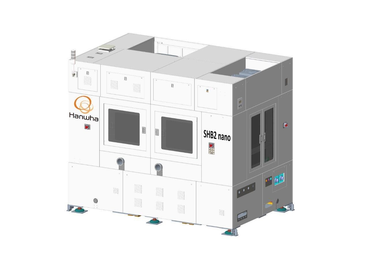
Hanwha Semitec’s second-generation hybrid bonder “SHB2 Nano.” Provided by Hanwha Semitec.
Hybrid bonding technology is seen as the solution that can overcome this limitation. It directly bonds chip to chip by joining copper pad to copper pad without bumps, effectively reducing the distance between DRAM dies to virtually “zero” and dramatically cutting overall thickness. This significantly increases data transfer speed and improves power efficiency, leading to expectations that it will become a “game changer” for the future semiconductor industry. According to global market research firm TechInsights, the hybrid bonder market is projected to grow to USD 1.6 billion (approximately KRW 2.407 trillion) by 2033. The industry expects that this technology will be adopted in earnest starting with HBM4E or HBM5, which are likely to use stacking structures of 20 layers or more.
To preempt this market, Hanwha Semitec established an “Advanced Packaging Equipment Development Center,” a dedicated organization for developing next-generation semiconductor equipment, and has concentrated on new technologies such as hybrid bonding. In 2022 it developed its first-generation hybrid bonder “SHB1” and supplied it to customers, and in February this year it completed development of the second-generation hybrid bonder “SHB2 Nano.”
SHB2 Nano controls positional error within a tolerance of 0.1 micrometers (μm). This is roughly one-thousandth the thickness of a human hair. Such ultra-fine accuracy is the key competitive edge of hybrid bonding technology, enabling chips to be stacked to improve performance while reducing overall semiconductor thickness.
Hanwha Semitec plans to supply SHB2 Nano to customers in the first half of this year and begin quality testing. The test results are expected to take about one year. The company anticipates that hybrid bonders will be adopted within the next two to three years.
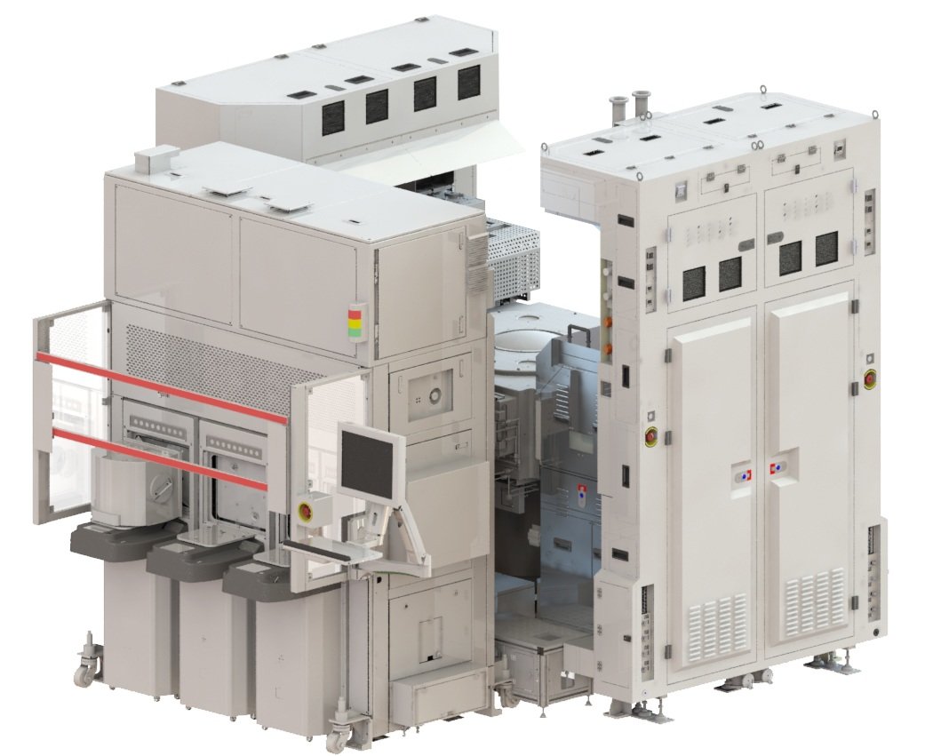
Hanwha Semitec ALD equipment “I2FIT.” Provided by Hanwha Semitec.
Another pillar of Hanwha Semitec’s efforts to leap forward as a “comprehensive semiconductor equipment manufacturer” is the front-end process segment. In 2024, Hanwha Semitec reportedly supplied key front-end demo equipment, including ALD (atomic layer deposition) and PECVD (plasma-enhanced chemical vapor deposition), to customers’ semiconductor research centers, where they are undergoing quality evaluation.
The front-end equipment market has higher entry barriers than the back-end equipment market. Demo testing typically takes more than two years, and even after passing the qual test, additional verification steps are required before equipment can be deployed on mass production lines. However, if it passes the qual test, the company is expected to evolve into a comprehensive semiconductor equipment manufacturer covering both front-end and back-end processes.
“Independence declaration” by Kim Dong-seon, expanding into semiconductors… “Targeting the market with ultra-precision innovative technology”
Hanwha Semitec’s performance slowed in the first quarter of this year. It posted revenue of KRW 83.1 billion and an operating loss of KRW 13.7 billion, with revenue down 38.8% from the previous quarter and operating profit turning to a loss.
The market, however, views this as a temporary effect of customers holding off on new investment and suspending equipment orders ahead of the transition from HBM3E to HBM4. As HBM4 mass production ramps up in the second half, TC bonder orders are expected to rebound, increasing the likelihood of improved earnings.
Securities firms are also issuing optimistic forecasts that if hybrid bonding technology is applied to NAND and foundry packaging, a full-fledged earnings turnaround could begin from 2027. The company says new orders are continuing to flow in and expects a return to profitability after a period of stabilization.
Management’s commitment is strong. Currently, tech affiliates such as Hanwha Vision, Hanwha Momentum and Hanwha Robotics are led by Executive Vice President Kim Dong-seon, the third son of Chairman Kim Seung-youn, who serves as Head of Future Vision at Hanwha Vision.
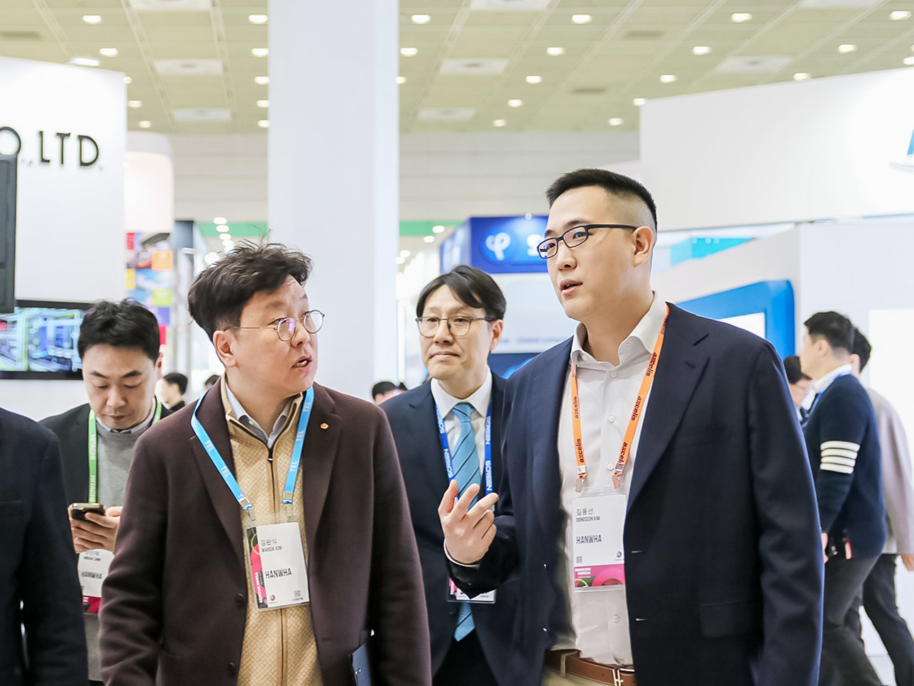
Kim Dong-seon, Executive Vice President and Head of Future Vision at Hanwha Vision, tours various parts of the Hanwha Semitec booth at SEMICON Korea 2025 to check on technology status. Provided by Hanwha Vision.
Executive Vice President Kim joined Hanwha Semitec as Head of Future Vision in February last year, announcing unpaid management and pledging a significant expansion in R&D (research and development) investment. He said, “In back-end areas such as HBM TC bonders, we are latecomers, but the only core of market competitiveness is innovative technology,” adding, “We will rapidly expand our market presence by leveraging Hanwha Semitec’s unique, unrivaled technologies.”
Hanwha Semitec’s R&D investment has indeed been steadily rising. According to its audit report, the company’s R&D expenditure over the past three years has increased from KRW 50.7 billion in 2023 to KRW 67.8 billion in 2024 and KRW 79.5 billion in 2025. Support from the parent company is also continuing. Hanwha Vision recently decided to participate in Hanwha Semitec’s rights offering and invest KRW 50 billion. The company described this as a strategic investment to expand its semiconductor equipment business.
In August, the tech and life segments of Hanwha Group are scheduled to be placed under a new holding company, tentatively named Hanwha Machinery & Service Holdings, through a spin-off. The structure will group tech affiliates such as Hanwha Vision, Hanwha Momentum, Hanwha Semitec and Hanwha Robotics, together with life affiliates such as Hanwha Galleria, Hanwha Hotels & Resorts and Our Home, under the new entity.
To focus on managing the holding company, Executive Vice President Kim resigned in March from his position as head of the overseas business division in the construction segment of Hanwha Corporation. Once the new holding company is launched, expectations are rising that investment and M&A decision-making will accelerate under his leadership. The market is watching closely to see whether Hanwha Vision, spearheaded by Hanwha Semitec, can make the leap to become a comprehensive semiconductor equipment company.
Hanwha Vision’s strategy in Q&A format
Q. Why has hybrid bonding not yet been applied to HBM?
Hybrid bonding is a next-generation bonding technology that directly joins copper interconnects on chip surfaces without bumps. It can dramatically narrow the gap between chips compared to TC bonding, and is therefore regarded as an essential technology for manufacturing highly stacked HBM with 20 layers or more.
However, there are many challenges to overcome before it can be commercialized. Because hybrid bonding directly connects copper interconnects, even minute alignment errors of several hundred nanometers (nm) or less can lead to open circuits or void formation.
Even if the technical issues are resolved, it will be difficult to survive in the market without cost-efficiency in mass production. Hybrid bonding is advantageous in wafer-to-wafer (W2W) mode, which bonds entire wafers, but if there are defective dies on the wafer, a fatal yield problem arises because good dies must be discarded along with the bad ones. In contrast, die-to-wafer (D2W) bonding, where dies are attached one by one, is hindered by low production speed. Ultimately, finding a balance between cost and yield on mass production lines is the key challenge for establishing this technology in the market.
Q. Why does the process become more complex as the number of HBM layers increases?
This is because the total chip thickness specification must be maintained while only increasing the number of layers. Under international semiconductor standards, HBM’s standard thickness is restricted. For HBM3 and earlier generations, it was around 720 μm, and for HBM4, which entered full-scale mass production early this year, it has increased to around 775 μm. To mass-produce highly stacked HBM with 16 to 20 layers, DRAM dies must be made even thinner, but as this approaches technical limits, the necessity of hybrid bonding is growing.
There are forecasts that the timing of hybrid bonding adoption could be somewhat delayed, as the JEDEC Solid State Technology Association is currently discussing relaxing height specifications. However, industry consensus is that as HBM advances, the adoption of hybrid bonding will ultimately become unavoidable. A Hanwha Semitec official stressed, “Regardless of any relaxation in standards, considering the efficiency of various back-end packaging technologies, the use of hybrid bonders will be essential in the future.”
Q. Can Hanwha Semitec evolve into a comprehensive semiconductor equipment company?
Hanwha Semitec is growing into the only company in Korea with both front-end and back-end
ⓒ dongA.com. All rights reserved. Reproduction, redistribution, or use for AI training prohibited.
Popular News











 About Dong-A Ilbo